- 您現在的位置:買賣IC網 > PDF目錄90604 > 10GL2CZ47A 10 A, 400 V, SILICON, RECTIFIER DIODE PDF資料下載
參數資料
| 型號: | 10GL2CZ47A |
| 元件分類: | 整流器 |
| 英文描述: | 10 A, 400 V, SILICON, RECTIFIER DIODE |
| 封裝: | 12-10C1A, 3 PIN |
| 文件頁數: | 1/5頁 |
| 文件大小: | 330K |
| 代理商: | 10GL2CZ47A |
10DL2CZ47A,10FL2CZ47A,10GL2CZ47A
2006-11-08
1
TOSHIBA HIGH EFFICIENCY DIODE STACK (HED) SILICON EPITAXIAL TYPE
10DL2CZ47A, 10FL2CZ47A, 10GL2CZ47A
SWITCHING MODE POWER SUPPLY APPLICATIONS
CONVERTER & CHOPPER APPLICATION
Repetitive Peak Reverse Voltage
: VRRM = 200 V, 300 V, 400 V
Average Output Rectified Current : IO = 10 A
Ultra Fast Reverse-Recovery Time : trr = 35 ns (Max)
Low Switching Losses and Output Noise
MAXIMUM RATINGS (Ta = 25°C)
CHARACTERISTIC
SYMBOL
RATING
UNIT
10DL2CZ47A
200
10FL2CZ47A
300
Repetitive Peak
Reverse Voltage
10GL2CZ47A
VRRM
400
V
Average Output Rectified Current
IO
10
A
50 (50Hz)
Peak One Cycle Surge Forward
Current (Sine Wave)
IFSM
55 (60Hz)
A
Junction Temperature
Tj
40~150
°C
Storage Temperature Range
Tstg
40~150
°C
Screw Torque
―
0.6
Nm
Note: Using continuously under heavy loads (e.g. the application of high temperature/current/voltage and the
significant change in temperature, etc.) may cause this product to decrease in the reliability significantly even
if the operating conditions (i.e. operating temperature/current/voltage, etc.) are within the absolute maximum
ratings.
Please design the appropriate reliability upon reviewing the Toshiba Semiconductor Reliability Handbook
(“Handling Precautions”/Derating Concept and Methods) and individual reliability data (i.e. reliability test report
and estimated failure rate, etc).
ELECTRICAL CHARACTERISTICS (Ta = 25°C)
CHARACTERISTIC
SYMBOL
TEST CONDITION
MIN.
TYP.
MAX.
UNIT
10DL2CZ47A
―
0.98
10FL2CZ47A
―
1.3
Peak Forward
Voltage
(Note 1)
10GL2CZ47A
VFM
IFM=5A
―
1.8
V
10DL2CZ47A
―
10
10FL2CZ47A
―
10
Repetitive Peak
Reverse Current
(Note 1)
10GL2CZ47A
IRRM
VRRM=Rated
―
50
A
Reverse Recovery Time
(Note 1)
trr
IF=2A, di / dt=20A / s
―
ns
Forward Recovery Time
(Note 1)
tfr
IF=1A
―
ns
Thermal Resistance
Rth (j-c)
Total DC, Junction to Case
―
°C / W
Note 1 : A value applied to one cell.
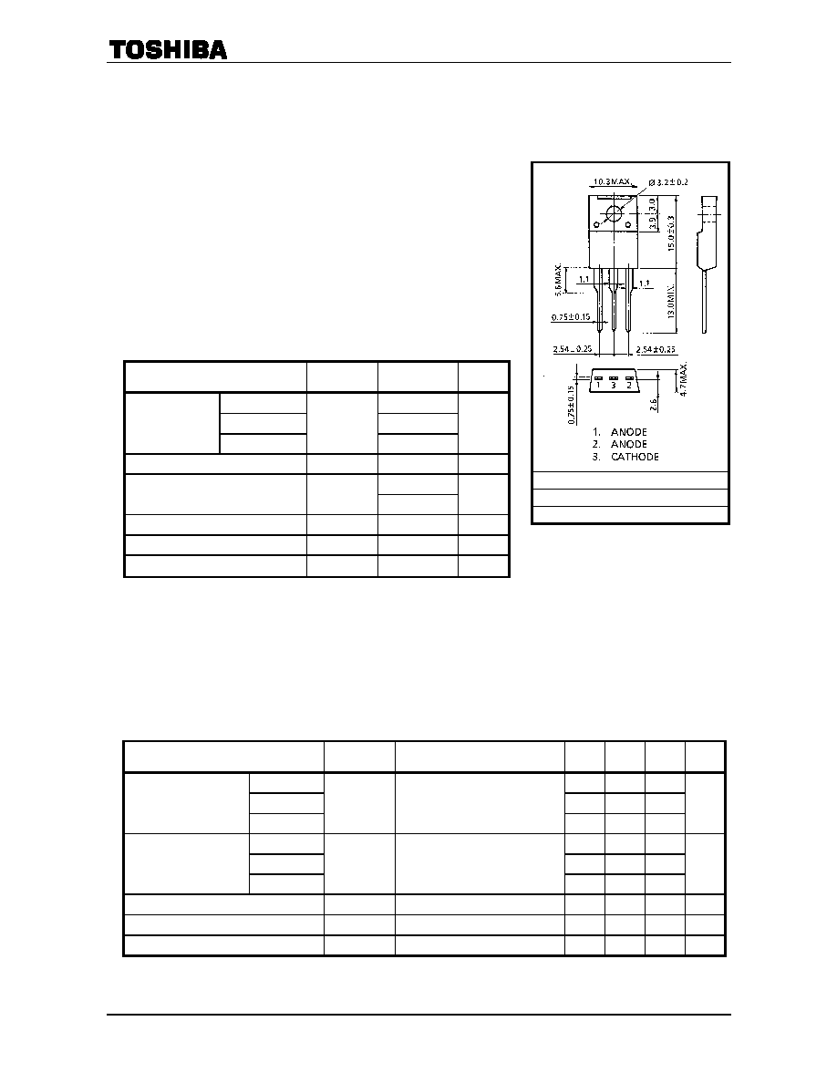
JEDEC
―
JEITA
―
TOSHIBA
12-10C1A
Weight : 2.0g
Unit in mm
相關PDF資料 |
PDF描述 |
|---|---|
| 10E2TA2B5 | 1 A, 200 V, SILICON, SIGNAL DIODE, DO-41 |
| 10E4TA2B5 | 1 A, 400 V, SILICON, SIGNAL DIODE, DO-41 |
| 10E8TR | 1 A, 800 V, SILICON, SIGNAL DIODE, DO-41 |
| 10E6 | 1 A, 600 V, SILICON, SIGNAL DIODE |
| 10EF1TA1B2 | 0.95 A, 100 V, SILICON, SIGNAL DIODE |
相關代理商/技術參數 |
參數描述 |
|---|---|
| 10GL2CZ47A(F) | 制造商:Toshiba America Electronic Components 功能描述:Diode Switching 400V 10A 3-Pin(3+Tab) TO-220NIS Bulk |
| 10G-PCI2-8C2L-2S+E | 制造商:Myricom 功能描述:MYRI10G "GEN2" (5GT/S) PCI EXPRESS NETWORK ADAPTER 20G B/S - Bulk |
| 10G-PCIE2-8C2-2S+DBL2 | 制造商:Myricom 功能描述:GEN3 2 CHIP PCI-EXPRESS ADD-IN CARD,STANDARD FACE PLATE DBL - Bulk |
| 10G-PCIE2-8C2-2S+SNF2+DBL2U | 制造商:Myricom 功能描述:10G-PCIE2-8C2-2S+SNF2+DBL2U - Bulk |
| 10G-PCIE2-8C2-2S-SYNC+SNF2+DBL | 制造商:Myricom 功能描述:10G-PCIE2-8C2-2S-SYNC+SNF2+DBL2U - Bulk |
發布緊急采購,3分鐘左右您將得到回復。