- 您現(xiàn)在的位置:買賣IC網(wǎng) > PDF目錄373914 > AD7712AN (ANALOG DEVICES INC) LC2MOS Signal Conditioning ADC PDF資料下載
參數(shù)資料
| 型號(hào): | AD7712AN |
| 廠商: | ANALOG DEVICES INC |
| 元件分類: | ADC |
| 英文描述: | LC2MOS Signal Conditioning ADC |
| 中文描述: | 2-CH 24-BIT DELTA-SIGMA ADC, SERIAL ACCESS, PDIP24 |
| 封裝: | 0.300 INCH, PLASTIC, DIP-24 |
| 文件頁數(shù): | 23/28頁 |
| 文件大小: | 229K |
| 代理商: | AD7712AN |
第1頁第2頁第3頁第4頁第5頁第6頁第7頁第8頁第9頁第10頁第11頁第12頁第13頁第14頁第15頁第16頁第17頁第18頁第19頁第20頁第21頁第22頁當(dāng)前第23頁第24頁第25頁第26頁第27頁第28頁
2
–23–
REV. E
AD7712
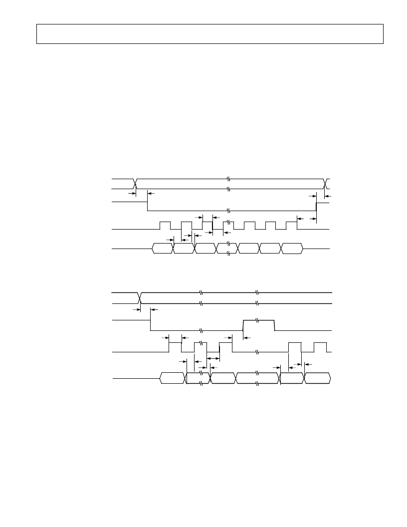
Write Operation
Data can be written to either the control register or calibration
registers. In either case, the write operation is not affected by
the
DRDY
line, and the write operation does not have any effect
on the status of
DRDY
. A write operation to the control regis-
ter or the calibration register must always write 24 bits to the
respective register.
Figure 14a shows a write operation to the AD7712 with
TFS
remaining low for the duration of the write operation. A0 deter-
mines whether a write operation transfers data to the control
register or to the calibration registers. This A0 signal must
remain valid for the duration of the serial write operation. As
before, the serial clock line should be low between read and
write operations. The serial data to be loaded to the AD7712
must be valid on the high level of the externally applied SCLK
signal. Data is clocked into the AD7712 on the high level of this
SCLK signal with the MSB transferred first. On the last active
high time of SCLK, the LSB is loaded to the AD7712.
Figure 14b shows a timing diagram for a write operation to the
AD7712 with
TFS
returning high during the write operation
and returning low again to write the rest of the data word. Tim-
ing parameters and functions are very similar to that outlined for
Figure 14a, but Figure 14b has a number of additional times to
show timing relationships when
TFS
returns high in the middle
of transferring a word.
Data to be loaded to the AD7712 must be valid prior to the
rising edge of the SCLK signal.
TFS
should return high during
the low time of SCLK. After
TFS
returns low again, the next bit
of the data word to be loaded to the AD7712 is clocked in on
next high level of the SCLK input. On the last active high time
of the SCLK input, the LSB is loaded to the AD7712.
SCLK (I)
SDATA (I)
TFS
(I)
A0 (I)
MSB
LSB
t
32
t
33
t
26
t
27
t
35
t
36
t
34
Figure 14a. External Clocking Mode, Control/Calibration Register Write Operation
SCLK (I)
SDATA (I)
TFS
(I)
A0 (I)
MSB
BIT N
BIT N+1
t
32
t
26
t
30
t
35
t
27
t
36
t
35
t
36
Figure 14b. External Clocking Mode, Control/Calibration Register Write Operation (
TFS
Returns High During
Write Operation)
相關(guān)PDF資料 |
PDF描述 |
|---|---|
| AD7712AQ | LC2MOS Signal Conditioning ADC |
| AD7712AR | LC2MOS Signal Conditioning ADC |
| AD7712SQ | LC2MOS Signal Conditioning ADC |
| AD7712* | Rail-to-Rail, Very Low Noise Universal Dual Filter Building Block; Package: SSOP; No of Pins: 16; Temperature Range: 0°C to +70°C |
| AD7712 | Signal Conditioning ADC(LC2MOS信號(hào)調(diào)節(jié)A/D轉(zhuǎn)換器) |
相關(guān)代理商/技術(shù)參數(shù) |
參數(shù)描述 |
|---|---|
| AD7712ANZ | 功能描述:IC ADC SIGNAL COND LC2MOS 24-DIP RoHS:是 類別:集成電路 (IC) >> 數(shù)據(jù)采集 - 模數(shù)轉(zhuǎn)換器 系列:- 其它有關(guān)文件:TSA1204 View All Specifications 標(biāo)準(zhǔn)包裝:1 系列:- 位數(shù):12 采樣率(每秒):20M 數(shù)據(jù)接口:并聯(lián) 轉(zhuǎn)換器數(shù)目:2 功率耗散(最大):155mW 電壓電源:模擬和數(shù)字 工作溫度:-40°C ~ 85°C 安裝類型:表面貼裝 封裝/外殼:48-TQFP 供應(yīng)商設(shè)備封裝:48-TQFP(7x7) 包裝:Digi-Reel® 輸入數(shù)目和類型:4 個(gè)單端,單極;2 個(gè)差分,單極 產(chǎn)品目錄頁面:1156 (CN2011-ZH PDF) 其它名稱:497-5435-6 |
| AD7712ANZ | 制造商:Analog Devices 功能描述:IC ADC 24-BIT SIGMA DELTA |
| AD7712AQ | 制造商:Rochester Electronics LLC 功能描述:24 BIT SIGMA DELTA ADC IC - Bulk |
| AD7712AR | 功能描述:IC ADC SIGNAL COND LC2MOS 24SOIC RoHS:否 類別:集成電路 (IC) >> 數(shù)據(jù)采集 - 模數(shù)轉(zhuǎn)換器 系列:- 標(biāo)準(zhǔn)包裝:1 系列:- 位數(shù):14 采樣率(每秒):83k 數(shù)據(jù)接口:串行,并聯(lián) 轉(zhuǎn)換器數(shù)目:1 功率耗散(最大):95mW 電壓電源:雙 ± 工作溫度:0°C ~ 70°C 安裝類型:通孔 封裝/外殼:28-DIP(0.600",15.24mm) 供應(yīng)商設(shè)備封裝:28-PDIP 包裝:管件 輸入數(shù)目和類型:1 個(gè)單端,雙極 |
| AD7712AR-REEL | 制造商:Analog Devices 功能描述:ADC Single Delta-Sigma 1.028ksps 24-bit Serial 24-Pin SOIC W T/R 制造商:Analog Devices 功能描述:ADC SGL DELTA-SIGMA 1.028KSPS 24BIT SERL 24SOIC W - Tape and Reel |
發(fā)布緊急采購,3分鐘左右您將得到回復(fù)。