- 您現在的位置:買賣IC網 > PDF目錄373917 > AD7804 (Analog Devices, Inc.) +3.3 V to +5 V Quad/Octal 10-Bit DACs PDF資料下載
參數資料
| 型號: | AD7804 |
| 廠商: | Analog Devices, Inc. |
| 英文描述: | +3.3 V to +5 V Quad/Octal 10-Bit DACs |
| 中文描述: | 3.3伏至5伏四/八通道10位DAC |
| 文件頁數: | 10/28頁 |
| 文件大小: | 300K |
| 代理商: | AD7804 |
第1頁第2頁第3頁第4頁第5頁第6頁第7頁第8頁第9頁當前第10頁第11頁第12頁第13頁第14頁第15頁第16頁第17頁第18頁第19頁第20頁第21頁第22頁第23頁第24頁第25頁第26頁第27頁第28頁
AD7804/AD7805/AD7808/AD7809
REV. A
–10–
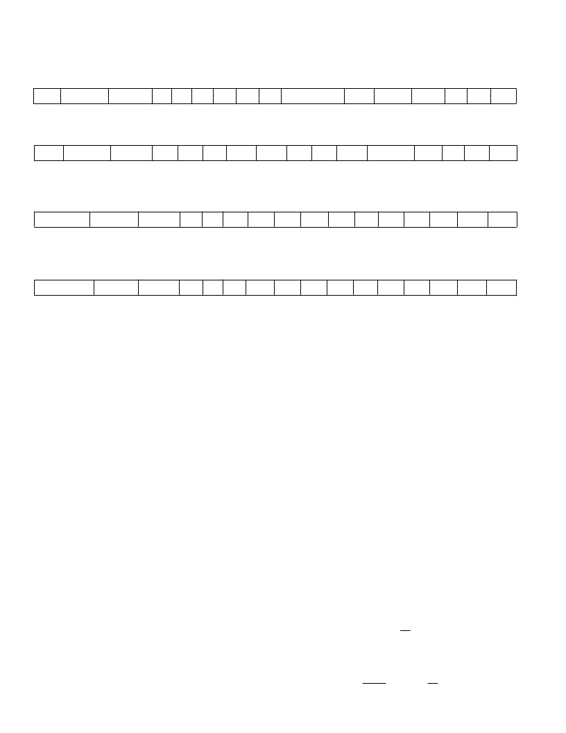
DB15 (MSB)
DB0 (LSB)
X
MD0 = 1
MD1 = 0
A2*
A1
A0
MX1
MX0
X
X
X
STBY
CLR
0
X
X
X = Don’t Care
*Applicable to the AD7808 Only, and Are Don’t Care Conditions when Operating the AD7804.
Figure 5. AD7804/AD7808 Channel Control Register Loading Sequence
DB15 (MSB)
DB0 (LSB)
MAIN
/SUB
MD0 = X
MD1 = 1 A2* A1
A0
DB9
DB8
DB7
DB6 DB5
DB4
DB3
DB2
DB1
DB0
X = Don’t Care
*Applicable to the AD7808 Only, and Are Don’t Care Conditions when Operating the AD7804.
Figure 6. AD7804/AD7808 Main DAC Data Register Loading Sequence (
MAIN
/SUB = 0)
DB15 (MSB)
DB0 (LSB)
MAIN
/SUB
MD0 = X
MD1 = 1 A2* A1
A0
DB7
DB6
DB5
DB4 DB3
DB2
DB1
DB0
X
X
X = Don’t Care
*Applicable to the AD7808 Only, and Are Don’t Care Conditions when Operating the AD7804.
Figure 7. AD7804/AD7808 Sub DAC Data Register Loading Sequence (
MAIN
/SUB = 1)
MSB
LSB
X
MD0 = 0
MD1 = 0
X
X
X
X
X
0
BIN
/
COMP
PD
SSTBY
SCLR 0 X
X
X = Don’t Care
Figure 4. AD7804/AD7808 System Control Register Loading Sequence
AD7804/AD7808 SYSTEM CONTROL REGISTER (MD1 = 0,
MD0 = 0)
The bits in this register allow control over all DACs in the
package. The control bits include power down (
PD
), DAC input
coding select (BIN/
COMP
), system standby (SSTBY) and a
system clear (SCLR). The function of these bits is as follows:
Power Down
(PD)
This bit in the control register is used to shut down the complete
device. With a 0 in this position, the reference and all DACs are
put into low power mode. Writing a 1 to this bit puts the part in
the normal operating mode. When in power-down mode, the
contents of all registers are retained and are valid when the
device is put back into normal operation.
Coding (BIN/
COMP
)
This bit in the system control register allows the user to select
one of two input coding schemes. The available schemes are
Twos complement coding and offset binary coding. All DACs
will be configured with the same input coding scheme. Writing
a zero to the control register selects twos complement coding,
while writing a 1 to this bit in the control register selects offset
binary coding.
With twos complement coding selected the output voltage from
the Main DAC is of the form :
V
OUT
=
V
BIAS
±
V
SWING
where
V
SWING
is
15
16
×
V
BIAS
With Offset Binary coding selected the output voltage from the
Main DAC ranges from:
V
OUT
=
V
BIAS
16
toV
OUT
=
31
16
×
V
BIAS
When the system control register is selected by writing zeros to
the mode bits, MD1 and MD0 the address bits are ignored as
the system control register controls all DACs in the package.
When MD1 = 0 and MD0 = 1, writing is to the channel control
register. Only the DAC selected by the address bits will be af-
fected by writing to this register. Each individual DAC has a
channel control register.
The DACs data registers are addressed by writing a one to
MD1 (DB13); the condition of MD0 (DB14) does not matter
when writing to the data registers. DB15 determines whether
writing is to the Main DAC data register or to the Sub DAC
data register. The Main DAC is 10 bits wide and the Sub DAC
is 8 bits wide. Thus when writing to the Sub DAC DB1 and
DB0 become don’t cares. The Sub DAC is used to offset the
complete transfer function of the Main DAC around its V
BIAS
point. The Sub DAC has 1/8 LSB resolution and will enable the
transfer function of the Main DAC to be offset by
±
V
BIAS
/32.
When the
LDAC
line goes low, all DAC registers in the device
are simultaneously loaded with the contents of their respective
DAC data registers, and the outputs change accordingly.
Bringing the
CLR
line low resets the DAC data and DAC regis-
ters. This hardware clear affects both the Main and Sub DACs.
This operation sets the analog output of the Main DAC to V
BIAS
/
16 when offset binary coding is selected and the output is set to
V
BIAS
when twos complement coding is used. V
BIAS
is the output
of the internal multiplexer as shown in Figure 3. The output of
the Sub DAC is used to shift the transfer function of the Main
DAC around the V
BIAS
point and the contribution from the Sub
DAC is zero following an external hardware clear. Software
clears affect the Main DACs only
.
相關PDF資料 |
PDF描述 |
|---|---|
| AD7804BN | ECONOLINE: REC2.2-S_DRW(Z)/H* - 2.2W DIP Package- 1kVDC Isolation- Regulated Output- 4.5-9V, 9-18V, 18-36V, 36-72V Wide Input Range 2 : 1- UL94V-0 Package Material- Continuous Short Circiut Protection- Cost Effective- 100% Burned In- Efficiency to 84% |
| AD7804BR | +3.3 V to +5 V Quad/Octal 10-Bit DACs |
| AD7805BN | %2B3.3V to %2B5V Quad/Octal 10-Bit DACs |
| AD7805BR | %2B3.3V to %2B5V Quad/Octal 10-Bit DACs |
| AD7805BRS | +3.3 V to +5 V Quad/Octal 10-Bit DACs |
相關代理商/技術參數 |
參數描述 |
|---|---|
| AD7804BN | 制造商:Analog Devices 功能描述:DAC 4-CH 10-bit 16-Pin PDIP Tube 制造商:Rochester Electronics LLC 功能描述:QUAD 10-BIT SERIAL DAC - Bulk |
| AD7804BNZ | 功能描述:IC DAC 10BIT QUAD SERIAL 16DIP RoHS:是 類別:集成電路 (IC) >> 數據采集 - 數模轉換器 系列:- 產品培訓模塊:Data Converter Fundamentals DAC Architectures 標準包裝:750 系列:- 設置時間:7µs 位數:16 數據接口:并聯 轉換器數目:1 電壓電源:雙 ± 功率耗散(最大):100mW 工作溫度:0°C ~ 70°C 安裝類型:表面貼裝 封裝/外殼:28-LCC(J 形引線) 供應商設備封裝:28-PLCC(11.51x11.51) 包裝:帶卷 (TR) 輸出數目和類型:1 電壓,單極;1 電壓,雙極 采樣率(每秒):143k |
| AD7804BR | 功能描述:IC DAC 10BIT 3.3V QUAD 16-SOIC RoHS:否 類別:集成電路 (IC) >> 數據采集 - 數模轉換器 系列:- 產品培訓模塊:Data Converter Fundamentals DAC Architectures 標準包裝:750 系列:- 設置時間:7µs 位數:16 數據接口:并聯 轉換器數目:1 電壓電源:雙 ± 功率耗散(最大):100mW 工作溫度:0°C ~ 70°C 安裝類型:表面貼裝 封裝/外殼:28-LCC(J 形引線) 供應商設備封裝:28-PLCC(11.51x11.51) 包裝:帶卷 (TR) 輸出數目和類型:1 電壓,單極;1 電壓,雙極 采樣率(每秒):143k |
| AD7804BR-REEL | 功能描述:IC DAC 10BIT QUAD SRL 16-SOIC RoHS:否 類別:集成電路 (IC) >> 數據采集 - 數模轉換器 系列:- 標準包裝:47 系列:- 設置時間:2µs 位數:14 數據接口:并聯 轉換器數目:1 電壓電源:單電源 功率耗散(最大):55µW 工作溫度:-40°C ~ 85°C 安裝類型:表面貼裝 封裝/外殼:28-SSOP(0.209",5.30mm 寬) 供應商設備封裝:28-SSOP 包裝:管件 輸出數目和類型:1 電流,單極;1 電流,雙極 采樣率(每秒):* |
| AD7804BRZ | 功能描述:IC DAC 10BIT QUAD SRL 16-SOIC RoHS:是 類別:集成電路 (IC) >> 數據采集 - 數模轉換器 系列:- 標準包裝:1 系列:- 設置時間:4.5µs 位數:12 數據接口:串行,SPI? 轉換器數目:1 電壓電源:單電源 功率耗散(最大):- 工作溫度:-40°C ~ 125°C 安裝類型:表面貼裝 封裝/外殼:8-SOIC(0.154",3.90mm 寬) 供應商設備封裝:8-SOICN 包裝:剪切帶 (CT) 輸出數目和類型:1 電壓,單極;1 電壓,雙極 采樣率(每秒):* 其它名稱:MCP4921T-E/SNCTMCP4921T-E/SNRCTMCP4921T-E/SNRCT-ND |
發布緊急采購,3分鐘左右您將得到回復。