- 您現在的位置:買賣IC網 > PDF目錄373917 > AD7816ARM (Analog Devices, Inc.) Single- and 4-Channel, 9 us, 10-Bit ADCs with On-Chip Temperature Sensor PDF資料下載
參數資料
| 型號: | AD7816ARM |
| 廠商: | Analog Devices, Inc. |
| 元件分類: | 溫度/濕度傳感器 |
| 英文描述: | Single- and 4-Channel, 9 us, 10-Bit ADCs with On-Chip Temperature Sensor |
| 中文描述: | 與單核和4通道,9我們,10位ADC片上溫度傳感器 |
| 文件頁數: | 8/20頁 |
| 文件大小: | 279K |
| 代理商: | AD7816ARM |
REV. C
–8–
AD7816/AD7817/AD7818
AD7817 PIN FUNCTION DESCRIPTIONS
Pin
Mnemonic
Description
1
CONVST
Logic Input Signal. The convert start signal. A 10-bit analog-to-digital conversion is initiated on the
falling edge of this signal. The falling edge of this signal places the track/hold in hold mode. The track/
hold goes into track mode again at the end of the conversion. The state of the
CONVST
signal is checked
at the end of a conversion. If it is logic low, the AD7817 will power-down—see Operating Mode section
of the data sheet.
Logic Output. The busy signal is logic high during a temperature or voltage A/D conversion. The signal
can be used to interrupt a microcontroller when a conversion has finished.
Logic Output. The Overtemperature Indicator (
OTI
) is set logic low if the result of a conversion on
Channel 0 (Temperature Sensor) is greater that an 8-bit word in the Overtemperature Register (OTR).
The signal is reset at the end of a serial read operation, i.e., a rising RD/
WR
edge when
CS
is low.
Logic Input Signal. The chip select signal is used to enable the serial port of the AD7817. This is neces-
sary if the AD7817 is sharing the serial bus with more than one device.
Analog Ground. Ground reference for track/hold, comparator and capacitor DAC.
Analog Input. An external 2.5 V reference can be connected to the AD7817 at this pin. To enable the on-
chip reference the REF
IN
pin should be tied to AGND. If an external reference is connected to the
AD7817, the internal reference will shut down.
Analog Input Channels. The AD7817 has four analog input channels. The input channels are single-
ended with respect to AGND (analog ground). The input channels can convert voltage signals in the
range 0 V to V
REF
. A channel is selected by writing to the Address Register of the AD7817—see Control
Byte section.
Positive Supply Voltage, 2.7 V to 5.5 V.
Digital Ground. Ground reference for digital circuitry.
Logic Output With a High Impedance State. Data is clocked out of the AD7817 serial port at this pin.
This output goes into a high impedance state on the falling edge of RD/
WR
or on the rising edge of the
CS
signal, whichever occurs first.
Logic Input. Data is clocked into the AD7817 at this pin.
Clock Input for the Serial Port. The serial clock is used to clock data into and out of the AD7817. Data is
clocked out on the falling edge and clocked in on the rising edge.
Logic Input Signal. The read/write signal is used to indicate to the AD7817 whether the data transfer
operation is a read or a write. The RD/
WR
should be set logic high for a read operation and logic low for
a write operation.
2
BUSY
3
OTI
4
CS
5
6
AGND
REF
IN
7–10
V
IN1
to V
IN4
11
12
13
V
DD
DGND
D
OUT
14
15
D
IN
SCLK
16
RD/
WR
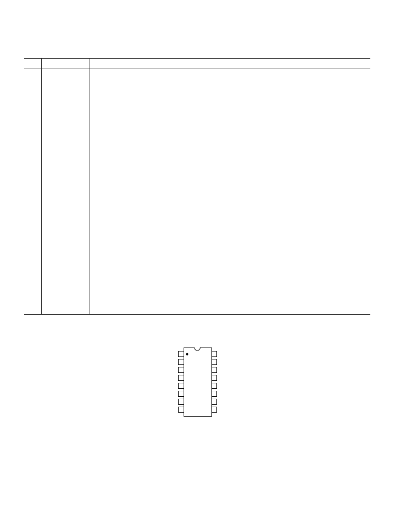
PIN CONFIGURATION
SOIC/TSSOP
14
13
12
11
16
15
10
9
8
1
2
3
4
7
6
5
TOP VIEW
(Not to Scale)
AD7817
CONVST
D
OUT
D
IN
SCLK
RD/
WR
BUSY
O T I
CS
V
IN4
V
IN3
V
DD
DGND
AGND
REF
IN
V
IN1
V
IN2
相關PDF資料 |
PDF描述 |
|---|---|
| AD7818AR | Single- and 4-Channel, 9 us, 10-Bit ADCs with On-Chip Temperature Sensor |
| AD7818ARM | Single- and 4-Channel, 9 us, 10-Bit ADCs with On-Chip Temperature Sensor |
| AD7816AR-REEL7 | Single- and 4-Channel, 9 us, 10-Bit ADCs with On-Chip Temperature Sensor |
| AD7818AR-REEL7 | Single- and 4-Channel, 9 us, 10-Bit ADCs with On-Chip Temperature Sensor |
| AD7819YN | +2.7 V to +5.5 V, 200 kSPS 8-Bit Sampling ADC |
相關代理商/技術參數 |
參數描述 |
|---|---|
| AD7816ARM-REEL | 制造商:Analog Devices 功能描述:Analog Temperature Sensors 8-Pin MSOP T/R 制造商:Rochester Electronics LLC 功能描述:TEMPERATURE SENSOR: 10-BIT ADC, TEMPERATURE MONITORING ONLY - Tape and Reel |
| AD7816ARM-REEL7 | 制造商:Analog Devices 功能描述:Analog Temperature Sensors 8-Pin MSOP T/R |
| AD7816ARMZ | 制造商:Analog Devices 功能描述:Analog Temperature Sensors 8-Pin MSOP |
| AD7816ARMZ-REEL | 制造商:Analog Devices 功能描述:Analog Temperature Sensors 8-Pin MSOP T/R 制造商:Analog Devices 功能描述:ANLG TEMP SENSORS 8MSOP - Tape and Reel |
| AD7816ARMZ-REEL7 | 制造商:Analog Devices 功能描述:Analog Temperature Sensors 8-Pin MSOP T/R 制造商:Analog Devices 功能描述:ANLG TEMP SENSORS 8MSOP - Tape and Reel |
發布緊急采購,3分鐘左右您將得到回復。