- 您現在的位置:買賣IC網 > PDF目錄373917 > AD7823YR (ANALOG DEVICES INC) 1.2V, 12 Bit 200KSPS, Serial ADC 6-SOT-23 -40 to 85 PDF資料下載
參數資料
| 型號: | AD7823YR |
| 廠商: | ANALOG DEVICES INC |
| 元件分類: | ADC |
| 英文描述: | 1.2V, 12 Bit 200KSPS, Serial ADC 6-SOT-23 -40 to 85 |
| 中文描述: | 1-CH 8-BIT SUCCESSIVE APPROXIMATION ADC, SERIAL ACCESS, PDSO8 |
| 封裝: | SOIC-8 |
| 文件頁數: | 3/11頁 |
| 文件大小: | 155K |
| 代理商: | AD7823YR |
AD7823
–3–
REV. B
TIMING CHARACTERISTICS
1, 2
Parameter
V
DD
= 5 V 10%
V
DD
= 3 V 10%
Unit
Conditions/Comments
t
1
t
2
t
3
t
4
t
53
t
63
t
73
t
83, 4
5
20
25
25
5
10
5
20
10
1
5
20
25
25
5
10
5
20
10
1
μ
s (max)
ns (min)
ns (min)
ns (min)
ns (min)
ns (max)
ns (max)
ns (max)
ns (min)
μ
s (max)
Conversion Time Mode 1 Operation (High Speed Mode)
CONVST
Pulsewidth
SCLK High Pulsewidth
SCLK Low Pulsewidth
CONVST
Rising Edge to SCLK Rising Edge Set-Up Time
SCLK Rising Edge to D
OUT
Data Valid Delay
Data Hold Time after Rising Edge SCLK
Bus Relinquish Time After Falling Edge of SCLK
t
POWERUP
Power-Up Time
NOTES
1
Sample tested to ensure compliance.
2
See Figures 14, 15 and 16.
3
These numbers are measured with the load circuit of Figure 1. They are defined as the time required for the o/p to cross 0.8 V or 2.4 V for V
DD
= 5 V
±
10% and
0.4 V or 2 V for V
= 3 V
±
10%.
4
Derived from the measured time taken by the data outputs to change 0.5 V when loaded with the circuit of Figure 1. The measured number is then extrapolated back
to remove the effects of charging or discharging the 50 pF capacitor. This means that the time quoted in the Timing Characteristics, t
8
, is the true bus relinquish time
of the part and as such is independent of external bus loading capacitances.
Specifications subject to change without notice.
(–40 C to +125 C, unless otherwise noted)
ABSOLUTE MAXIMUM RATINGS*
(T
A
= +25
°
C unless otherwise noted)
V
DD
to GND . . . . . . . . . . . . . . . . . . . . . . . . . . –0.3 V to +7 V
Digital Input Voltage to GND
(
CONVST
, SCLK) . . . . . . . . . . . . . . –0.3 V, V
DD
+ 0.3 V
Digital Output Voltage to GND
(D
OUT
) . . . . . . . . . . . . . . . . . . . . . . . . . –0.3 V, V
DD
+ 0.3 V
V
REF
to GND . . . . . . . . . . . . . . . . . . . . . . –0.3 V, V
DD
+ 0.3 V
Analog Inputs
(V
IN +
, V
IN –
) . . . . . . . . . . . . . . . . . . . . . –0.3 V, V
DD
+ 0.3 V
Storage Temperature Range . . . . . . . . . . . . –65
°
C to +150
°
C
Junction Temperature . . . . . . . . . . . . . . . . . . . . . . . . .+150
°
C
Plastic DIP Package, Power Dissipation . . . . . . . . . . 450 mW
θ
JA
Thermal Impedance . . . . . . . . . . . . . . . . . . . +125
°
C/W
θ
JC
Thermal Impedance . . . . . . . . . . . . . . . . . . . . +50
°
C/W
Lead Temperature, Soldering (10 sec) . . . . . . . . . . +260
°
C
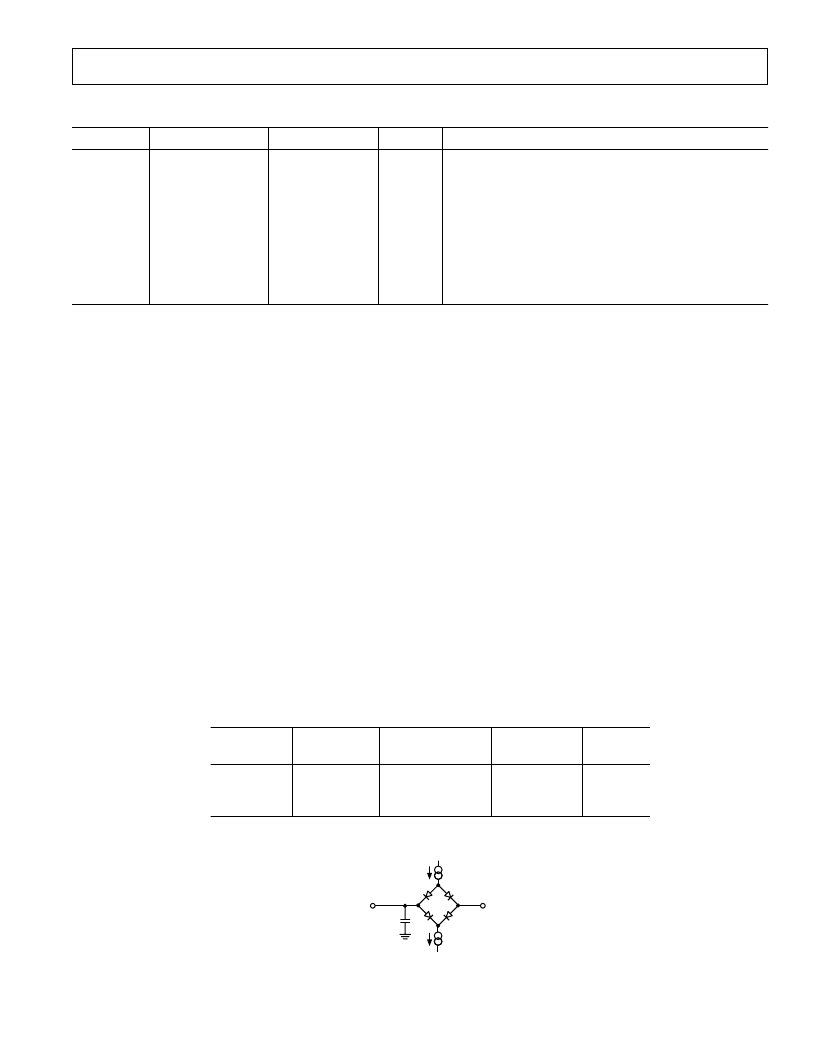
I
OL
200mA
I
200 A
1.6V
C
L
50pF
TO
OUTPUT
PIN
Figure 1. Load Circuit for Digital Output Timing Specifications
SOIC Package, Power Dissipation . . . . . . . . . . . . . . . 450 mW
θ
JA
Thermal Impedance . . . . . . . . . . . . . . . . . . . . 160
°
C/W
θ
JC
Thermal Impedance . . . . . . . . . . . . . . . . . . . . . 56
°
C/W
Lead Temperature, Soldering
Vapor Phase (60 sec) . . . . . . . . . . . . . . . . . . . . . .+215
°
C
Infrared (15 sec) . . . . . . . . . . . . . . . . . . . . . . . . . .+220
°
C
MicroSOIC Package, Power Dissipation . . . . . . . . . . 450 mW
θ
JA
Thermal Impedance . . . . . . . . . . . . . . . . . . . . 206
°
C/W
θ
JC
Thermal Impedance . . . . . . . . . . . . . . . . . . . . . 44
°
C/W
Lead Temperature, Soldering
Vapor Phase (60 sec) . . . . . . . . . . . . . . . . . . . . . .+215
°
C
Infrared (15 sec) . . . . . . . . . . . . . . . . . . . . . . . . . .+220
°
C
*Stresses above those listed under Absolute Maximum Ratings may cause perma-
nent damage to the device. This is a stress rating only; functional operation of the
device at these or any other conditions above those listed in the operational sections
of this specification is not implied. Exposure to absolute maximum rating condi-
tions for extended periods may affect device reliability.
ORDERING GUIDE
Linearity
Error
Temperature
Range
Branding
Information
Package
Option*
Model
AD7823YN
AD7823YR
AD7823YRM
±
1 LSB
±
1 LSB
±
1 LSB
–40
°
C to +125
°
C
–40
°
C to +125
°
C
–40
°
C to +125
°
C
N-8
SO-8
RM-8
C2Y
*N = plastic DIP; RM = microSOIC; SO = small outline IC (SOIC).
相關PDF資料 |
PDF描述 |
|---|---|
| AD7825 | 3 V/5 V, 2 MSPS, 8-Bit, 1-, 4-, 8-Channel Sampling ADCs |
| AD7825BN | 3 V/5 V, 2 MSPS, 8-Bit, 1-, 4-, 8-Channel Sampling ADCs |
| AD7825BR | 3 V/5 V, 2 MSPS, 8-Bit, 1-, 4-, 8-Channel Sampling ADCs |
| AD7825BRU | 14-Bit 48KSPS DAS with ADC, MUX, PGA and Internal Reference 28-SSOP -40 to 85 |
| AD7822BN | 3 V/5 V, 2 MSPS, 8-Bit, 1-, 4-, 8-Channel Sampling ADCs |
相關代理商/技術參數 |
參數描述 |
|---|---|
| AD7823YRM | 制造商:Analog Devices 功能描述:ADC Single SAR 200ksps 8-bit Serial 8-Pin MSOP 制造商:Rochester Electronics LLC 功能描述:8-BIT SERIAL SINGLE ADC I.C. - Bulk 制造商:Analog Devices 功能描述:IC 8-BIT ADC |
| AD7823YRM-REEL | 制造商:Analog Devices 功能描述:ADC Single SAR 200ksps 8-bit Serial 8-Pin MSOP T/R 制造商:Analog Devices 功能描述:ADC SGL SAR 200KSPS 8BIT SERL 8MSOP - Tape and Reel |
| AD7823YRM-REEL7 | 制造商:Analog Devices 功能描述:ADC Single SAR 200ksps 8-bit Serial 8-Pin MSOP T/R 制造商:Rochester Electronics LLC 功能描述:8-BIT SERIAL SINGLE ADC I.C. - Tape and Reel |
| AD7823YRMZ | 功能描述:IC ADC 8BIT SRL 2.7-5.5V 8MSOP RoHS:是 類別:集成電路 (IC) >> 數據采集 - 模數轉換器 系列:- 其它有關文件:TSA1204 View All Specifications 標準包裝:1 系列:- 位數:12 采樣率(每秒):20M 數據接口:并聯 轉換器數目:2 功率耗散(最大):155mW 電壓電源:模擬和數字 工作溫度:-40°C ~ 85°C 安裝類型:表面貼裝 封裝/外殼:48-TQFP 供應商設備封裝:48-TQFP(7x7) 包裝:Digi-Reel® 輸入數目和類型:4 個單端,單極;2 個差分,單極 產品目錄頁面:1156 (CN2011-ZH PDF) 其它名稱:497-5435-6 |
| AD7823YRMZ-REEL | 功能描述:IC ADC 8BIT SRL 2.7-5.5V 8MSOP RoHS:是 類別:集成電路 (IC) >> 數據采集 - 模數轉換器 系列:- 標準包裝:2,500 系列:- 位數:16 采樣率(每秒):15 數據接口:MICROWIRE?,串行,SPI? 轉換器數目:1 功率耗散(最大):480µW 電壓電源:單電源 工作溫度:-40°C ~ 85°C 安裝類型:表面貼裝 封裝/外殼:38-WFQFN 裸露焊盤 供應商設備封裝:38-QFN(5x7) 包裝:帶卷 (TR) 輸入數目和類型:16 個單端,雙極;8 個差分,雙極 配用:DC1011A-C-ND - BOARD DELTA SIGMA ADC LTC2494 |
發布緊急采購,3分鐘左右您將得到回復。