- 您現在的位置:買賣IC網 > PDF目錄373918 > AD7847 (Analog Devices, Inc.) LC2MOS Complete, Dual 12-Bit MDACs PDF資料下載
參數資料
| 型號: | AD7847 |
| 廠商: | Analog Devices, Inc. |
| 英文描述: | LC2MOS Complete, Dual 12-Bit MDACs |
| 中文描述: | LC2MOS完成,雙12位醫療儀器行政管理制度 |
| 文件頁數: | 9/12頁 |
| 文件大小: | 187K |
| 代理商: | AD7847 |
AD7837/AD7847
REV. C
–9–
APPLICATIONS
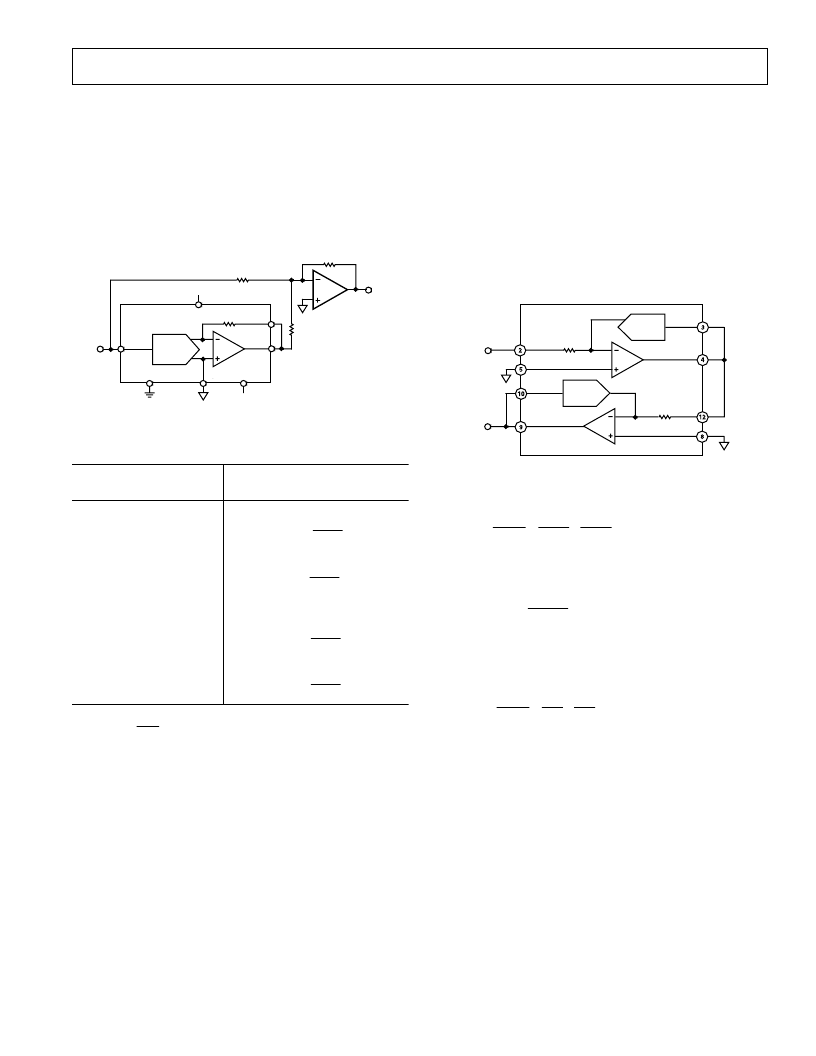
PROGRAMMABLE GAIN AMPLIFIER (PGA)
The dual DAC/amplifier combination along with access to R
FB
make the AD7837 ideal as a programmable gain amplifier. In this
application, the DAC functions as a programmable resistor in the
amplifier feedback loop. This type of configuration is shown
in Figure 17 and is suitable for ac gain control. The circuit con-
sists of two PGAs in series. Use of a dual configuration provides
greater accuracy over a wider dynamic range than a single PGA
solution. The overall system gain is the product of the individual
gain stages. The effective gains for each stage are controlled by
the DAC codes. As the code decreases, the effective DAC
resistance increases, and so the gain also increases.
DAC B
AGNDA
V
OUTB
V
REFB
V
IN
R
FBB
AD7837
V
OUT
R
FBA
AGNDB
DAC A
V
OUTA
V
REFA
Figure 17. Dual PGA Circuit
The transfer function is given by
V
OUT
V
IN
=
R
EQA
R
FBA
×
R
EQB
R
FBB
(1)
where
R
EQA
,
R
EQB
are the effective DAC resistances controlled
by the digital input code:
R
EQ
=
2
12
R
IN
N
(2)
where
R
IN
is the DAC input resistance and is equal to R
FB
and
N
= DAC input code in decimal.
The transfer function in (1) thus simplifies to
V
OUT
V
IN
=
2
12
N
A
×
2
12
N
B
(3)
where
N
A
= DAC A input code in decimal and
N
B
= DAC B
input code in decimal.
N
A
, N
B
may be programmed between 1 and (2
12
–
1). The zero
code is not allowed as it results in an open loop amplifier
response. To minimize errors, the digital codes N
A
and N
B
should be chosen to be equal to or as close as possible to each
other to achieve the required gain.
BIPOLAR OPERATION
(4-QUADRANT MULTIPLICATION)
Figure 16 shows the AD7837/AD7847 connected for bipolar
operation. The coding is offset binary as shown in Table IV.
When V
IN
is an ac signal, the circuit performs 4-quadrant multi-
plication. To maintain the gain error specifications, resistors R1,
R2 and R3 should be ratio matched to 0.01%. Note that on the
AD7847 the feedback resistor R
FB
is internally connected to
V
OUT
.
DAC A
AGNDA
V
OUTA
V
REFA
V
IN
DGND
V
SS
R
FBA
*
V
DD
V
DD
AD7837
AD7847
*
INTERNALLY
CONNECTED
ON AD7847
R3
10k
R1
20k
AD711
R2
20k
V
OUT
V
SS
Figure 16. Bipolar Offset Binary Operation
Table IV. Bipolar Code Table
DAC Latch Contents
MSB LSB
Analog Output, V
OUT
1111 1111 1111
+
V
IN
×
2047
2048
1000 0000 0001
0 V
+
V
IN
×
1
2048
1000 0000 0000
0111 1111 1111
–
V
IN
×
1
2048
0000 0000 0000
–
V
IN
×
2048
2048
=
–
V
IN
Note 1 LSB =
V
IN
2048
.
相關PDF資料 |
PDF描述 |
|---|---|
| AD7847AN | LC2MOS Complete, Dual 12-Bit MDACs |
| AD7847AQ | LC2MOS Complete, Dual 12-Bit MDACs |
| AD7847AR | LC2MOS Complete, Dual 12-Bit MDACs |
| AD7847BN | LC2MOS Complete, Dual 12-Bit MDACs |
| AD7847BQ | LC2MOS Complete, Dual 12-Bit MDACs |
相關代理商/技術參數 |
參數描述 |
|---|---|
| AD7847AN | 功能描述:IC DAC 12BIT MULT DUAL 24-DIP RoHS:否 類別:集成電路 (IC) >> 數據采集 - 數模轉換器 系列:- 產品培訓模塊:Data Converter Fundamentals DAC Architectures 標準包裝:750 系列:- 設置時間:7µs 位數:16 數據接口:并聯 轉換器數目:1 電壓電源:雙 ± 功率耗散(最大):100mW 工作溫度:0°C ~ 70°C 安裝類型:表面貼裝 封裝/外殼:28-LCC(J 形引線) 供應商設備封裝:28-PLCC(11.51x11.51) 包裝:帶卷 (TR) 輸出數目和類型:1 電壓,單極;1 電壓,雙極 采樣率(每秒):143k |
| AD7847AN/883B | 制造商:AD 制造商全稱:Analog Devices 功能描述:LC2MOS Complete, Dual 12-Bit MDACs |
| AD7847AN883B | 制造商:AD 制造商全稱:Analog Devices 功能描述:LC2MOS Complete, Dual 12-Bit MDACs |
| AD7847AN-883B | 制造商:AD 制造商全稱:Analog Devices 功能描述:LC2MOS Complete, Dual 12-Bit MDACs |
| AD7847ANN | 制造商:AD 制造商全稱:Analog Devices 功能描述:LC2MOS Complete, Dual 12-Bit MDACs |
發布緊急采購,3分鐘左右您將得到回復。