- 您現在的位置:買賣IC網 > PDF目錄373928 > AD8011 (Analog Devices, Inc.) 300 MHz, 1 mA Current Feedback Amplifier PDF資料下載
參數資料
| 型號: | AD8011 |
| 廠商: | Analog Devices, Inc. |
| 英文描述: | 300 MHz, 1 mA Current Feedback Amplifier |
| 中文描述: | 300兆赫,1 mA電流反饋放大器 |
| 文件頁數: | 12/16頁 |
| 文件大小: | 219K |
| 代理商: | AD8011 |
REV. B
–12–
AD8011
11
10
9
8
7
5
4
3
6
2
1
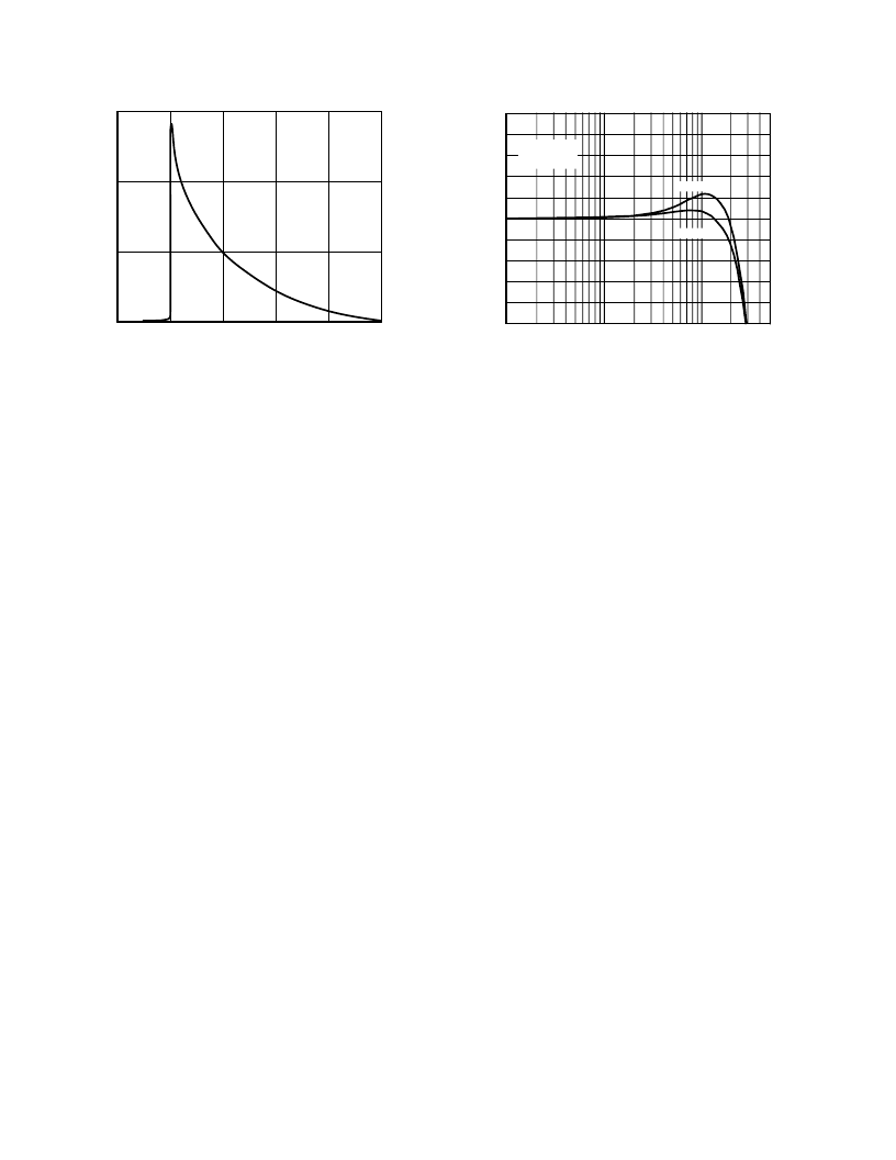
1 10 100 500
FREQUENCY
–
MHz
G
–
R
F
= 1k
R
F
= 750
V
= 5V
G = +2
V
IN
= 200mV
Figure 35. Flatness vs. Feedback
Output pin and external component capacitance (designated
C
L
) will further extend the devices BW and can also cause peak-
ing below and above the CLBW if too high. In the time domain,
poor step settling characteristics (ringing up to about 2 GHz
and excessive overshoot) can result. For high C
L
values greater
than about 5 pF an external series
“
damping
”
resistor is recom-
mended. See section on Settling Time vs. C
L
. For light loads,
any output capacitance will reflect back on A2
’
s output (Z2 of
buffer A3) as both added capacitance near the CLBW (CLBW
> f
T
/B) and eventually negative resistance at much higher fre-
quencies. These added effects are proportional to the load C.
This reflected capacitance and negative resistance has the effect
of both reducing A2/s phase margin and causing high frequency
“
L
×
C
”
peaking respectively. Using an external series resistor
(as specified above) reduces these unwanted effects by creating a
reflected zero to A2
’
s output which will reduce the peaking and
eliminate ringing. For heavy resistive loads, relatively more Load
C would be required to cause these same effects.
High inductive parasitics, especially on the supplies and inverting/
noninverting inputs, can cause modulated low level R
F
ringing
on the output in the transient domain. Again, proper R
F
compo-
nent and board layout practices need to be observed. Relatively
high parasitic lead inductance (roughly L >15 nh) can result in
L
×
C underdamped ringing. Here L/C means all associated
input pin, external component and leadframe strays including
collector to substrate device capacitance. In the ac domain, this
L
×
C resonance effect would typically not appear in the pass-
band of the amplifier but would appear in the open loop re-
sponse at frequencies well above the CLBW of the amplifier.
40
30
20
0
10
15
20
25
C
L
–
pF
10
R
S
–
5
Figure 34. Recommended R
SERIES
vs. Capacitive Load for
≤
30 ns Settling to 0.1%
OPTIMIZING FLATNESS
As mentioned, the ac transfer equations above are based on
a simplified single pole model. Due to the devices internal para-
sitics (primarily CP1/CP1B and CP2 in Figure 28) and
external package/board parasites (partially represented in Figure
34) the computed BW, using the V
O
(s) equation above, typi-
cally will be lower than the AD8011
’
s measured small signal
BW. See data sheet Bode plots.
With internal parasitics included only, the BW is extended do to
the complex pole pairs created primarily by CP1/CP2B and CP2
versus the single-pole assumption shown above. This results in a
“
design controlled
”
closed-loop damping factor (
ζ)
of nominally
0.6 resulting in the CLBW increasing by approximately 1.3
×
higher than the computed single pole value above
for optimized
external gains of +2/–1
! As external noninverting gain (G) is
increased, the actual closed-loop bandwidth vs. the computed
single pole ac response is in closer agreement.
Inverting pin and external component capacitance (designated
C
P
) will further extend the CLBW do the closed loop zero cre-
ated by C
P
and R
N
R
F
when operating in the noninverting mode.
Using proper R
F
component and layout techniques (see layout
section) this capacitance should be about 1.5 pF. This results in a
further incremental BW increase of almost 2
×
(versus the com-
puted value) for G = +1 decreasing and approaching its complex
pole pair BW for gains approaching +6 or higher. As previously
discussed, the single-pole response begins to correlate well. Note
that a pole is also created by 1/2 g
mf
and C
P
which prevents the
AD8011 from becoming unstable. This parasitic has the greatest
effect on BW and peaking for low positive gains as the data
sheet Bode plots clearly show. For inverting operation, C
P
has
relatively much less effect on CLBW variation.
相關PDF資料 |
PDF描述 |
|---|---|
| AD8011* | Micropower Op Amp, Comparator and Reference; Package: MSOP; No of Pins: 8; Temperature Range: 0°C to +70°C |
| AD8011-EB | 300 MHz, 1 mA Current Feedback Amplifier |
| AD8011AN | 300 MHz, 1 mA Current Feedback Amplifier |
| AD8011AR | 300 MHz, 1 mA Current Feedback Amplifier |
| AD8011AR-REEL7 | 300 MHz, 1 mA Current Feedback Amplifier |
相關代理商/技術參數 |
參數描述 |
|---|---|
| AD8011_03 | 制造商:AD 制造商全稱:Analog Devices 功能描述:300 MHz Current Feedback Amplifier |
| AD80112 | 制造商:Analog Devices 功能描述:N/A - Bulk |
| AD80113 | 制造商:Analog Devices 功能描述:N/A - Bulk |
| AD80115BCPZ | 制造商:Analog Devices 功能描述: |
發布緊急采購,3分鐘左右您將得到回復。