- 您現在的位置:買賣IC網 > PDF目錄373942 > AD8303 (Analog Devices, Inc.) Dual, Serial Input Complete 12-Bit DAC(串行輸入雙12位D/A轉換器) PDF資料下載
參數資料
| 型號: | AD8303 |
| 廠商: | Analog Devices, Inc. |
| 英文描述: | Dual, Serial Input Complete 12-Bit DAC(串行輸入雙12位D/A轉換器) |
| 中文描述: | 雙通道,串行輸入完整的12位DAC(串行輸入雙12位的D / A轉換器) |
| 文件頁數: | 5/16頁 |
| 文件大小: | 378K |
| 代理商: | AD8303 |
AD8303
REV. 0
–5–
Table I. Control-Logic Truth Table
CS
CLK
RS
MSB
SHDN LDA/B
Serial Shift Register Function
DAC Register Function
H
L
L
L
↑
+
H
H
X
X
X
X
X
X
L
H
↑
+
L
X
X
X
X
X
X
X
H
H
H
H
H
H
H
L
↑
+
L
↑
+
X
X
X
X
X
X
X
X
H
H
L
X
X
H
H
H
H
H
H
H
H
H
H
H
L
H
H
H
H
H
↓
–
L
X
H
X
H
X
No Effect
No Effect
No Effect
Shift-Register-Data Advanced One Bit Latched
No Effect
No Effect
No Effect
No Effect
No Effect
No Effect
No Effect
No Effect
Latched
Latched
Latched
Latched
Updated with Current Shift Register Contents
Transparent
Loaded with 800
H
Latched with 800
H
Loaded with All Zeros
Latched All Zeros
No Effect
NOTES
1
↑
+ positive logic transition;
↓
– negative logic transition; X Don’t Care.
2
Do not clock in serial data while
LDA
or
LDB
is LOW.
PIN DESCRIPTIONS
Pin No.
Name
Function
1
2
AGND
V
OUTA
Analog Ground.
DAC voltage output, 2.0475 V full scale with 0.5 mV per bit. An internal temperature stabilized reference
maintains a fixed full-scale voltage independent of time, temperature and power supply variations.
Reference Voltage Output Terminal. Very high output resistance must be buffered if used as a virtual
ground.
Digital Ground
Chip Select, Active Low Input. Disables shift register loading when high. Does not effect
LDA
or
LDB
operation.
Clock Input, positive edge clocks data into shift register.
Serial Data Input, input data loads directly into the shift register.
Load DAC register strobes, active low. Transfers shift register data to DAC A register. Asynchronous active
low input. See Control Logic Truth Table for operation.
Resets DAC register to zero condition or half-scale depending on MSB pin. Asynchronous active low input.
Load DAC register strobes, active low. Transfers shift register data to DAC B register. Asynchronous active
low input. See Control Logic Truth Table for operation.
Digital Input: Logic High presets DAC registers to half-scale 800
H
(sets MSB bit to one) when the
RS
pin
is strobed; Logic Low clears all DAC registers to zero (000
H
) when the
RS
pin is strobed.
Active low shutdown control input. Does not affect register contents as long as power is present on V
DD
.
Positive power supply input. Specified range of operation +2.7 V to +5.5 V
DAC voltage output, 2.0475 V full scale with 0.5 mV per bit. An internal temperature stabilized reference
maintains a fixed full-scale voltage independent of time, temperature and power supply variations.
3
V
REF
4
5
DGND
CS
6
7
8
CLK
SDI
LDA
9
10
RS
LDB
11
MSB
12
13
14
SHDN
V
DD
V
OUTB
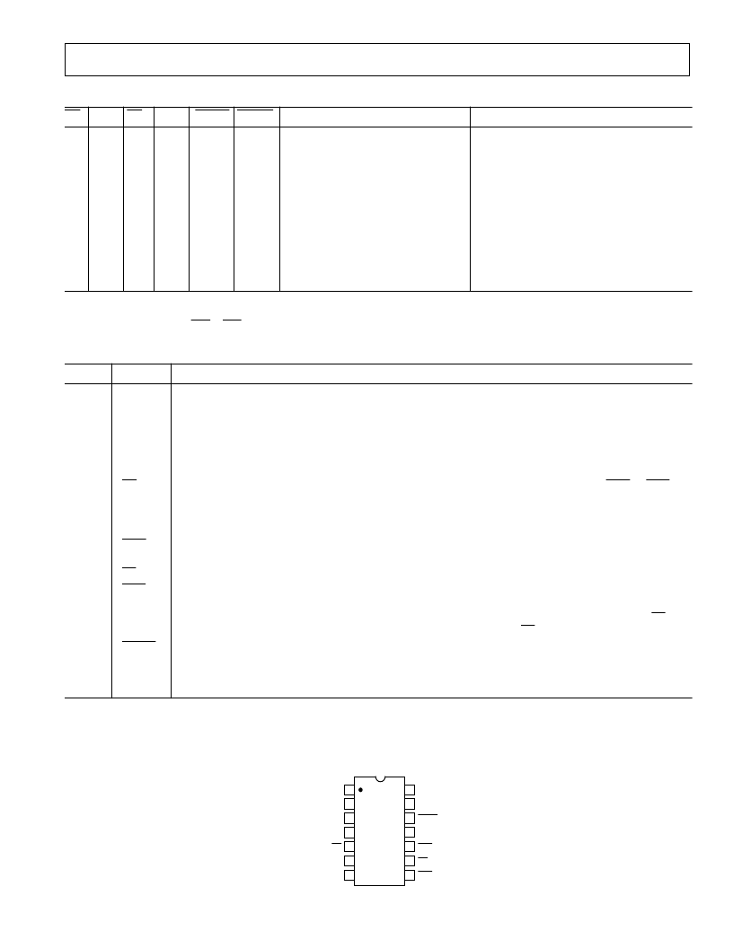
PIN CONFIGURATION
14-Pin P-DIP (N-14)
14-Lead SOIC (R-14)
14
13
12
11
10
9
8
1
2
3
4
7
6
5
TOP VIEW
(Not to Scale)
AGND
MSB
SHDN
V
DD
V
OUTB
V
OUTA
V
REF
DGND
AD8303
LDA
RS
LDB
CS
CLK
SDI
相關PDF資料 |
PDF描述 |
|---|---|
| AD8304ARU-REEL | 160 dB Range (100 pA -10 mA) Logarithmic Converter |
| AD8304 | 160 dB Range (100 pA -10 mA) Logarithmic Converter |
| AD8304-EVAL | 160 dB Range (100 pA -10 mA) Logarithmic Converter |
| AD8304ARU | 160 dB Range (100 pA -10 mA) Logarithmic Converter |
| AD8304ARU-REEL7 | 160 dB Range (100 pA -10 mA) Logarithmic Converter |
相關代理商/技術參數 |
參數描述 |
|---|---|
| AD8303AN | 制造商:AD 制造商全稱:Analog Devices 功能描述:+3 V, Dual, Serial Input Complete 12-Bit DAC |
| AD8303AR | 制造商:Analog Devices 功能描述:IC 12-BIT DAC |
| AD8303AR-REEL | 制造商:Analog Devices 功能描述:DAC 2-CH R-2R 12-bit 14-Pin SOIC N T/R 制造商:Rochester Electronics LLC 功能描述:IC,DUAL 12BIT,+3V,COMPLETE DAC,TAPE&REEL - Tape and Reel |
| AD8303ARZ-REEL | 功能描述:IC DAC 12BIT SERIAL 14SOIC RoHS:是 類別:集成電路 (IC) >> 數據采集 - 數模轉換器 系列:- 標準包裝:2,400 系列:- 設置時間:- 位數:18 數據接口:串行 轉換器數目:3 電壓電源:模擬和數字 功率耗散(最大):- 工作溫度:-40°C ~ 85°C 安裝類型:表面貼裝 封裝/外殼:36-TFBGA 供應商設備封裝:36-TFBGA 包裝:帶卷 (TR) 輸出數目和類型:* 采樣率(每秒):* |
| AD8303JRU | 制造商:Analog Devices 功能描述:DAC 2-CH R-2R 12-bit 14-Pin TSSOP 制造商:Rochester Electronics LLC 功能描述:IC,DUAL 12BIT,+3V,COMPLETE DAC - Bulk |
發布緊急采購,3分鐘左右您將得到回復。