- 您現在的位置:買賣IC網 > PDF目錄373943 > AD8331-EVAL (Analog Devices, Inc.) Ultralow Noise VGAs with Preamplifier and Programmable RIN PDF資料下載
參數資料
| 型號: | AD8331-EVAL |
| 廠商: | Analog Devices, Inc. |
| 英文描述: | Ultralow Noise VGAs with Preamplifier and Programmable RIN |
| 中文描述: | 超低噪聲的VGA前置放大器和可編程與房地產經紀人 |
| 文件頁數: | 19/32頁 |
| 文件大小: | 482K |
| 代理商: | AD8331-EVAL |
第1頁第2頁第3頁第4頁第5頁第6頁第7頁第8頁第9頁第10頁第11頁第12頁第13頁第14頁第15頁第16頁第17頁第18頁當前第19頁第20頁第21頁第22頁第23頁第24頁第25頁第26頁第27頁第28頁第29頁第30頁第31頁第32頁
AD8331/AD8332
Rev. C | Page 19 of 32
V
OUT
UNTERMINATED
R
IN
+
–
V
IN
R
S
V
OUT
RESISTIVE TERMINATION
R
IN
R
S
+
–
V
IN
R
S
V
OUT
ACTIVE IMPEDANCE MATCH –R
S
= R
IN
R
IN
R
S
+
–
V
IN
R
FB
R
FB
1 + 4.5
R
IN
=
0
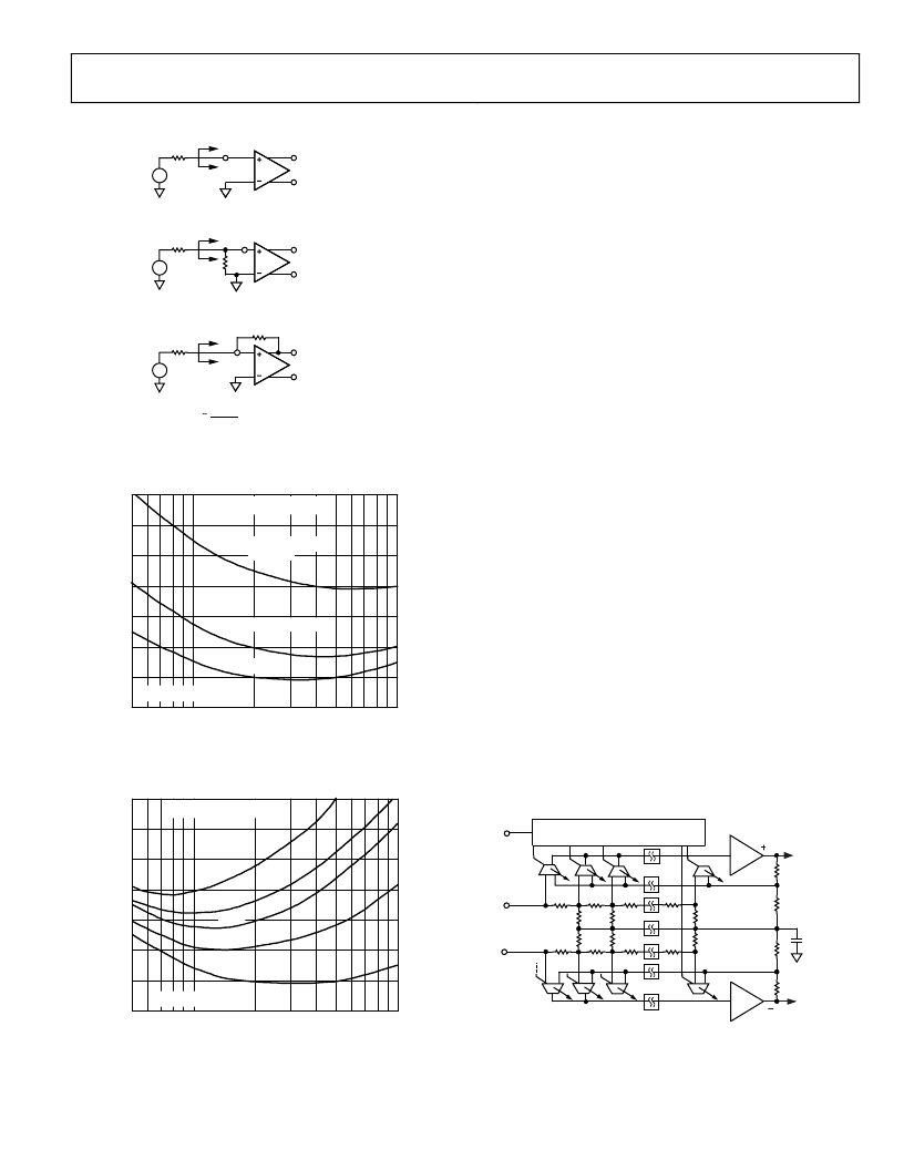
Figure 60. Input Configurations
N
5
6
7
4
2
1
3
0
100
50
1k
R
S
(
)
ACTIVE IMPEDANCE MATCH
RESISTIVE TERMINATION
(R
S
= R
IN
)
UNTERMINATED
SIMULATION
INCLUDES NOISE OF VGA
0
Figure 61. Noise Figure vs. R
S
for Resistive,
Active Matched, and Unterminated Inputs
N
5
6
7
4
2
1
3
0
100
50
1k
R
IN
= 50
70
R
FB
=
∞
R
S
(
)
200
INCLUDES NOISE OF VGA
100
SIMULATION
0
Figure 62. Noise Figure vs. R
S
for Various Fixed Values of R
IN
, Actively Matched
The primary purpose of input impedance matching is to
improve the system transient response. With resistive
termination, the input noise increases due to the thermal noise
of the matching resistor and the increased contribution of the
LNA’s input voltage noise generator. With active impedance
matching, however, the contributions of both are smaller than
they would be for resistive termination by a factor of 1/(1 +
LNA Gain
). Figure 61 shows their relative noise figure (NF)
performance. In this graph, the input impedance has been swept
with R
S
to preserve the match at each point. The noise figures
for a source impedance of 50 Ω are 7.1 dB, 4.1 dB, and 2.5 dB,
respectively, for the resistive, active, and unterminated
configurations. The noise figures for 200 Ω are 4.6 dB, 2.0 dB,
and 1.0 dB, respectively.
Figure 62 is a plot of the NF versus R
S
for various values of R
IN
,
which is helpful for design purposes. The plateau in the NF for
actively matched inputs mitigates source impedance variations.
For comparison purposes, a preamp with a gain of 19 dB and
noise spectral density of a 1.0 nV/√Hz, combined with a VGA
with 3.75 nV/√Hz, would yield a noise figure degradation of
approximately 1.5 dB (for most input impedances), significantly
worse than the AD8332 performance.
The equivalent input noise of the LNA is the same for single-
ended and differential output applications. The LNA noise
figure improves to 3.5 dB at 50 Ω without VGA noise, but this
is exclusive of noise contributions from other external circuits
connected to LOP. A series output resistor is usually
recommended for stability purposes, when driving external
circuits on a separate board (see the Applications section). In
low noise applications, a ferrite bead is even more desirable.
VARIABLE GAIN AMPLIFIER
The differential X-AMP VGA provides precise input
attenuation and interpolation. It has a low input-referred noise
of 2.7 nV/√Hz and excellent gain linearity. A simplified block
diagram is shown in Figure 63.
GAIN INTERPOLATOR
(BOTH CHANNELS)
POST-AMP
VIP
GAIN
R
6dB
2R
48dB
VIN
g
m
0
POST-AMP
Figure 63. Simplified VGA Schematic
相關PDF資料 |
PDF描述 |
|---|---|
| AD8331ARQ | Ultralow Noise VGAs with Preamplifier and Programmable RIN |
| AD8332 | Ultralow Noise VGAs with Preamplifier and Programmable RIN |
| AD8332-EVAL | Ultralow Noise VGAs with Preamplifier and Programmable RIN |
| AD8332ACP-REEL | Ultralow Noise VGAs with Preamplifier and Programmable RIN |
| AD8332ACP-REEL7 | Ultralow Noise VGAs with Preamplifier and Programmable RIN |
相關代理商/技術參數 |
參數描述 |
|---|---|
| AD8331-EVALZ | 功能描述:BOARD EVAL FOR AD8331 RoHS:是 類別:編程器,開發系統 >> 評估板 - 運算放大器 系列:X-AMP® 產品培訓模塊:Lead (SnPb) Finish for COTS Obsolescence Mitigation Program 標準包裝:1 系列:- |
| AD8331-EVALZ | 制造商:Analog Devices 功能描述:AD8331, VARIABLE GAIN AMPLIFIER, EVALUAT |
| AD8332 | 制造商:AD 制造商全稱:Analog Devices 功能描述:Ultralow Noise VGAs with Preamplifier and Programmable RIN |
| AD8332ACP-R2 | 功能描述:IC VGA DUAL W/PREAMP LN 32-LFCSP RoHS:否 類別:集成電路 (IC) >> 線性 - 放大器 - 專用 系列:X-AMP® 產品培訓模塊:Lead (SnPb) Finish for COTS Obsolescence Mitigation Program 標準包裝:60 系列:- 類型:可變增益放大器 應用:CATV 安裝類型:表面貼裝 封裝/外殼:20-WQFN 裸露焊盤 供應商設備封裝:20-TQFN-EP(5x5) 包裝:托盤 |
| AD8332ACP-REEL | 制造商:Analog Devices 功能描述:SP Amp Variable Gain Amp Dual 5.5V 32-Pin LFCSP EP T/R 制造商:Rochester Electronics LLC 功能描述: |
發布緊急采購,3分鐘左右您將得到回復。