參數資料
| 型號: | C8051F021 |
| 廠商: | Silicon Laboratories Inc |
| 文件頁數: | 91/272頁 |
| 文件大小: | 0K |
| 描述: | IC 8051 MCU 64K FLASH 64TQFP |
| 標準包裝: | 160 |
| 系列: | C8051F02x |
| 核心處理器: | 8051 |
| 芯體尺寸: | 8-位 |
| 速度: | 25MHz |
| 連通性: | EBI/EMI,SMBus(2 線/I²C),SPI,UART/USART |
| 外圍設備: | 欠壓檢測/復位,POR,PWM,溫度傳感器,WDT |
| 輸入/輸出數: | 32 |
| 程序存儲器容量: | 64KB(64K x 8) |
| 程序存儲器類型: | 閃存 |
| RAM 容量: | 4.25K x 8 |
| 電壓 - 電源 (Vcc/Vdd): | 2.7 V ~ 3.6 V |
| 數據轉換器: | A/D 8x8b,8x12b; D/A 2x12b |
| 振蕩器型: | 內部 |
| 工作溫度: | -40°C ~ 85°C |
| 封裝/外殼: | 64-TQFP |
| 包裝: | 托盤 |
第1頁第2頁第3頁第4頁第5頁第6頁第7頁第8頁第9頁第10頁第11頁第12頁第13頁第14頁第15頁第16頁第17頁第18頁第19頁第20頁第21頁第22頁第23頁第24頁第25頁第26頁第27頁第28頁第29頁第30頁第31頁第32頁第33頁第34頁第35頁第36頁第37頁第38頁第39頁第40頁第41頁第42頁第43頁第44頁第45頁第46頁第47頁第48頁第49頁第50頁第51頁第52頁第53頁第54頁第55頁第56頁第57頁第58頁第59頁第60頁第61頁第62頁第63頁第64頁第65頁第66頁第67頁第68頁第69頁第70頁第71頁第72頁第73頁第74頁第75頁第76頁第77頁第78頁第79頁第80頁第81頁第82頁第83頁第84頁第85頁第86頁第87頁第88頁第89頁第90頁當前第91頁第92頁第93頁第94頁第95頁第96頁第97頁第98頁第99頁第100頁第101頁第102頁第103頁第104頁第105頁第106頁第107頁第108頁第109頁第110頁第111頁第112頁第113頁第114頁第115頁第116頁第117頁第118頁第119頁第120頁第121頁第122頁第123頁第124頁第125頁第126頁第127頁第128頁第129頁第130頁第131頁第132頁第133頁第134頁第135頁第136頁第137頁第138頁第139頁第140頁第141頁第142頁第143頁第144頁第145頁第146頁第147頁第148頁第149頁第150頁第151頁第152頁第153頁第154頁第155頁第156頁第157頁第158頁第159頁第160頁第161頁第162頁第163頁第164頁第165頁第166頁第167頁第168頁第169頁第170頁第171頁第172頁第173頁第174頁第175頁第176頁第177頁第178頁第179頁第180頁第181頁第182頁第183頁第184頁第185頁第186頁第187頁第188頁第189頁第190頁第191頁第192頁第193頁第194頁第195頁第196頁第197頁第198頁第199頁第200頁第201頁第202頁第203頁第204頁第205頁第206頁第207頁第208頁第209頁第210頁第211頁第212頁第213頁第214頁第215頁第216頁第217頁第218頁第219頁第220頁第221頁第222頁第223頁第224頁第225頁第226頁第227頁第228頁第229頁第230頁第231頁第232頁第233頁第234頁第235頁第236頁第237頁第238頁第239頁第240頁第241頁第242頁第243頁第244頁第245頁第246頁第247頁第248頁第249頁第250頁第251頁第252頁第253頁第254頁第255頁第256頁第257頁第258頁第259頁第260頁第261頁第262頁第263頁第264頁第265頁第266頁第267頁第268頁第269頁第270頁第271頁第272頁
C8051F020/1/2/3
180
Rev. 1.4
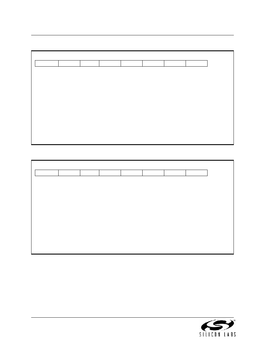
Figure 17.21. P4: Port4 Data Register
Bits7-0:
P4.[7:0]: Port4 Output Latch Bits.
Write - Output appears on I/O pins.
0: Logic Low Output.
1: Logic High Output (Open-Drain if corresponding P74OUT bit = 0). See Figure 17.20.
Read - Returns states of I/O pins.
0: P4.n pin is logic low.
1: P4.n pin is logic high.
Note: P4.7 (/WR), P4.6 (/RD), and P4.5 (ALE) can be driven by the External Data Memory Interface.
page 145 for more information.
R/W
Reset Value
P4.7
P4.6
P4.5
P4.4
P4.3
P4.2
P4.1
P4.0
11111111
Bit7
Bit6
Bit5
Bit4
Bit3
Bit2
Bit1
Bit0
SFR Address:
0x84
Figure 17.22. P5: Port5 Data Register
Bits7-0:
P5.[7:0]: Port5 Output Latch Bits.
Write - Output appears on I/O pins.
0: Logic Low Output.
1: Logic High Output (Open-Drain if corresponding P74OUT bit = 0). See Figure 17.20.
Read - Returns states of I/O pins.
0: P5.n pin is logic low.
1: P5.n pin is logic high.
Note:
P5.[7:0] can be driven by the External Data Memory Interface (as Address[15:8] in Non-multiplexed
on page 145 for more information about the External Memory Interface.
R/W
Reset Value
P5.7
P5.6
P5.5
P5.4
P5.3
P5.2
P5.1
P5.0
11111111
Bit7
Bit6
Bit5
Bit4
Bit3
Bit2
Bit1
Bit0
SFR Address:
0x85
相關PDF資料 |
PDF描述 |
|---|---|
| PIC18F4685-I/P | IC PIC MCU FLASH 48KX16 40DIP |
| C8051F020 | IC 8051 MCU 64K FLASH 100TQFP |
| C8051F016 | IC 8051 MCU 32K FLASH 48TQFP |
| C8051F015 | IC 8051 MCU 32K FLASH 64TQFP |
| C8051F236 | IC 8051 MCU 8K FLASH 48TQFP |
相關代理商/技術參數 |
參數描述 |
|---|---|
| C8051F021-GQ | 功能描述:8位微控制器 -MCU 64KB 12ADC 64P MCU RoHS:否 制造商:Silicon Labs 核心:8051 處理器系列:C8051F39x 數據總線寬度:8 bit 最大時鐘頻率:50 MHz 程序存儲器大小:16 KB 數據 RAM 大小:1 KB 片上 ADC:Yes 工作電源電壓:1.8 V to 3.6 V 工作溫度范圍:- 40 C to + 105 C 封裝 / 箱體:QFN-20 安裝風格:SMD/SMT |
| C8051F021-GQR | 功能描述:8位微控制器 -MCU 64KB 12ADC 64Pin MCU Tape and Reel RoHS:否 制造商:Silicon Labs 核心:8051 處理器系列:C8051F39x 數據總線寬度:8 bit 最大時鐘頻率:50 MHz 程序存儲器大小:16 KB 數據 RAM 大小:1 KB 片上 ADC:Yes 工作電源電壓:1.8 V to 3.6 V 工作溫度范圍:- 40 C to + 105 C 封裝 / 箱體:QFN-20 安裝風格:SMD/SMT |
| C8051F021R | 功能描述:8位微控制器 -MCU ADC 12/64Pin RoHS:否 制造商:Silicon Labs 核心:8051 處理器系列:C8051F39x 數據總線寬度:8 bit 最大時鐘頻率:50 MHz 程序存儲器大小:16 KB 數據 RAM 大小:1 KB 片上 ADC:Yes 工作電源電壓:1.8 V to 3.6 V 工作溫度范圍:- 40 C to + 105 C 封裝 / 箱體:QFN-20 安裝風格:SMD/SMT |
| C8051F022 | 功能描述:8位微控制器 -MCU 64KB 10ADC RoHS:否 制造商:Silicon Labs 核心:8051 處理器系列:C8051F39x 數據總線寬度:8 bit 最大時鐘頻率:50 MHz 程序存儲器大小:16 KB 數據 RAM 大小:1 KB 片上 ADC:Yes 工作電源電壓:1.8 V to 3.6 V 工作溫度范圍:- 40 C to + 105 C 封裝 / 箱體:QFN-20 安裝風格:SMD/SMT |
| C8051F022/0065 | 制造商:Silicon Laboratories Inc 功能描述: |
發布緊急采購,3分鐘左右您將得到回復。