- 您現在的位置:買賣IC網 > PDF目錄375765 > FDP8880 (FAIRCHILD SEMICONDUCTOR CORP) N-Channel PowerTrench MOSFET PDF資料下載
參數資料
| 型號: | FDP8880 |
| 廠商: | FAIRCHILD SEMICONDUCTOR CORP |
| 元件分類: | JFETs |
| 英文描述: | N-Channel PowerTrench MOSFET |
| 中文描述: | 11 A, 30 V, 0.0145 ohm, N-CHANNEL, Si, POWER, MOSFET, TO-220AB |
| 封裝: | TO-220AB, 3 PIN |
| 文件頁數: | 3/11頁 |
| 文件大小: | 231K |
| 代理商: | FDP8880 |
2005 Fairchild Semiconductor Corporation
FDP8880 / FDB8880 Rev. A
www.fairchildsemicom
F
3
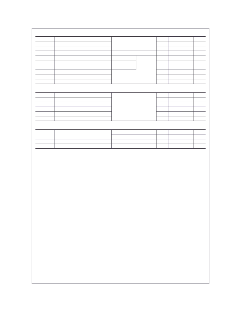
Dynamic Characteristics
C
ISS
Input Capacitance
C
OSS
Output Capacitance
C
RSS
Reverse Transfer Capacitance
R
G
Gate Resistance
Q
g(TOT)
Total Gate Charge at 10V
Q
g(5)
Total Gate Charge at 5V
Q
g(TH)
Threshold Gate Charge
Q
gs
Gate to Source Gate Charge
Q
gs2
Gate Charge Threshold to Plateau
Q
gd
Gate to Drain “Miller” Charge
Switching Characteristics
(V
GS
= 10V)
t
ON
Turn-On Time
t
d(ON)
Turn-On Delay Time
t
r
Rise Time
t
d(OFF)
Turn-Off Delay Time
t
f
Fall Time
t
OFF
Turn-Off Time
Drain-Source Diode Characteristics
Notes:
1:
Starting T
= 25°C, L = 34uH, I
AS
= 43A,Vdd = 27V, Vgs = 10V.
2:
Pulse width = 100s.
3:
FDP8880_NL / FDB8880_NL is lead free product.
FDP8880_NL / FDB8880_NL marking will appear on the reel label.
V
DS
= 15V, V
GS
= 0V,
f = 1MHz
-
-
-
-
-
-
-
-
-
-
1240
255
147
2.7
22
12
1.6
3.2
2.0
4.8
-
-
-
-
pF
pF
pF
nC
nC
nC
nC
nC
nC
V
GS
= 0.5V, f = 1MHz
V
GS
= 0V to 10V
V
GS
= 0V to 5V
V
GS
= 0V to 1V
V
DD
= 15V
I
D
= 40A
I
g
= 1.0mA
29
16
2.1
-
-
-
V
DD
= 15V, I
D
= 40A
V
GS
= 10V, R
GS
= 13.6
-
-
-
-
-
-
-
8
171
-
-
-
-
147
ns
ns
ns
ns
ns
ns
107
47
51
-
V
SD
Source to Drain Diode Voltage
I
SD
= 40A
I
SD
= 3.5A
I
SD
= 40A, dI
SD
/dt = 100A/
μ
s
I
SD
= 40A, dI
SD
/dt = 100A/
μ
s
-
-
-
-
-
-
-
-
1.25
1.0
27
18
V
V
ns
nC
t
rr
Q
RR
Reverse Recovery Time
Reverse Recovered Charge
相關PDF資料 |
PDF描述 |
|---|---|
| FDB8896 | N-Channel PowerTrench MOSFET 30V, 93A, 5.7 m ohm |
| FDC10-48S05W | 10 watts of output power from a 2 x 1 x 0.4 inch package |
| FDC10 | 10 watts of output power from a 2 x 1 x 0.4 inch package |
| FDC10-12D05 | 10 watts of output power from a 2 x 1 x 0.4 inch package |
| FDC10-12D12 | 10 watts of output power from a 2 x 1 x 0.4 inch package |
相關代理商/技術參數 |
參數描述 |
|---|---|
| FDP8880_08 | 制造商:FAIRCHILD 制造商全稱:Fairchild Semiconductor 功能描述:N-Channel PowerTrench㈢ MOSFET |
| FDP8896 | 功能描述:MOSFET 30V N-Channel PowerTrench RoHS:否 制造商:STMicroelectronics 晶體管極性:N-Channel 汲極/源極擊穿電壓:650 V 閘/源擊穿電壓:25 V 漏極連續電流:130 A 電阻汲極/源極 RDS(導通):0.014 Ohms 配置:Single 最大工作溫度: 安裝風格:Through Hole 封裝 / 箱體:Max247 封裝:Tube |
| FDP8896_08 | 制造商:FAIRCHILD 制造商全稱:Fairchild Semiconductor 功能描述:N-Channel PowerTrench㈢ MOSFET 30V, 92A, 5.9mヘ |
| FDP8896_F085 | 功能描述:MOSFET 30V N-Channel PowerTrench MOSFET. (Transferred to alternate site. Please contact local reps fo RoHS:否 制造商:STMicroelectronics 晶體管極性:N-Channel 汲極/源極擊穿電壓:650 V 閘/源擊穿電壓:25 V 漏極連續電流:130 A 電阻汲極/源極 RDS(導通):0.014 Ohms 配置:Single 最大工作溫度: 安裝風格:Through Hole 封裝 / 箱體:Max247 封裝:Tube |
| FDP8N50NZ | 功能描述:MOSFET UNIFET2 500V RoHS:否 制造商:STMicroelectronics 晶體管極性:N-Channel 汲極/源極擊穿電壓:650 V 閘/源擊穿電壓:25 V 漏極連續電流:130 A 電阻汲極/源極 RDS(導通):0.014 Ohms 配置:Single 最大工作溫度: 安裝風格:Through Hole 封裝 / 箱體:Max247 封裝:Tube |
發布緊急采購,3分鐘左右您將得到回復。