- 您現在的位置:買賣IC網 > PDF目錄375782 > FDS6162N7 (FAIRCHILD SEMICONDUCTOR CORP) 30V N-Channel PowerTrench MOSFET PDF資料下載
參數資料
| 型號: | FDS6162N7 |
| 廠商: | FAIRCHILD SEMICONDUCTOR CORP |
| 元件分類: | JFETs |
| 英文描述: | 30V N-Channel PowerTrench MOSFET |
| 中文描述: | 23 A, 20 V, 0.0035 ohm, N-CHANNEL, Si, POWER, MOSFET |
| 封裝: | FLMP, SO-8 |
| 文件頁數: | 2/6頁 |
| 文件大小: | 189K |
| 代理商: | FDS6162N7 |
FDS6162N3 Rev B2 (W)
Electrical Characteristics
T
A
= 25°C unless otherwise noted
Test Conditions
Symbol
Parameter
Min
Typ Max Units
Off Characteristics
BV
DSS
Drain–Source Breakdown
Voltage
Breakdown Voltage Temperature
Coefficient
Zero Gate Voltage Drain Current
Gate–Body Leakage, Forward
Gate–Body Leakage, Reverse
V
GS
= 0 V,
I
D
= 250
μ
A, Referenced to 25
°
C
V
DS
= 16 V,
V
GS
= 12 V,
V
GS
= –12 V ,
I
D
= 250
μ
A
20
V
BV
DSS
T
J
I
DSS
I
GSSF
I
GSSR
13
mV/
°
C
μ
A
nA
nA
V
GS
= 0 V
V
DS
= 0 V
V
DS
= 0 V
1
100
–100
On Characteristics
V
GS(th)
V
GS(th)
T
J
R
DS(on)
(Note 2)
Gate Threshold Voltage
Gate Threshold Voltage
Temperature Coefficient
Static Drain–Source
On–Resistance
V
DS
= V
GS
,
I
D
= 250
μ
A, Referenced to 25
°
C
V
GS
= 4.5 V, I
D
= 21 A
V
GS
= 2.5 V, I
D
= 18 A
V
GS
= 4.5 V, I
D
= 21 A, T
J
= 125
°
C
V
DS
= 5 V,
I
D
= 21 A
I
D
= 250
μ
A
0.6
0.9
–4
3.3
4.3
4.8
119
1.5
V
mV/
°
C
m
4.5
6.0
7.2
g
FS
Forward Transconductance
S
Dynamic Characteristics
C
iss
Input Capacitance
C
oss
Output Capacitance
C
rss
Reverse Transfer Capacitance
R
G
Gate Resistance
5521
1473
706
1.3
pF
pF
pF
V
DS
= 10 V,
f = 1.0 MHz
V
GS
= 0 V,
V
GS
= 15 mV,
f = 1.0 MHz
Switching Characteristics
(Note 2)
t
d(on)
Turn–On Delay Time
t
r
Turn–On Rise Time
t
d(off)
Turn–Off Delay Time
t
f
Turn–Off Fall Time
Q
g
Total Gate Charge
Q
gs
Gate–Source Charge
Q
gd
Gate–Drain Charge
20
25
85
55
52
9
14.5
32
40
136
88
73
ns
ns
ns
ns
nC
nC
nC
V
DD
= 10 V,
V
GS
= 4.5 V,
I
D
= 1 A,
R
GEN
= 6
V
DS
= 10 V,
V
GS
= 4.5 V
I
D
= 21 A,
Drain–Source Diode Characteristics and Maximum Ratings
I
S
Maximum Continuous Drain–Source Diode Forward Current
Drain–Source Diode Forward
Voltage
t
rr
Diode Reverse Recovery Time
Q
rr
Diode Reverse Recovery Charge
Notes:
2.5
1.2
A
V
nS
nC
V
SD
V
GS
= 0 V,
I
F
= 21 A,
d
iF
/d
t
= 100 A/μs
I
S
= 2.5 A
(Note 2)
0.6
42
52
1.
R
θ
JA
is the sum of the junction-to-case and case-to-ambient thermal resistance where the case thermal reference is defined as the solder mounting surface of
the drain pins. R
θ
JC
is guaranteed by design while R
θ
CA
is determined by the user's board design.
a)
40°C/W when
mounted on a 1in
2
pad
of 2 oz copper
b)
85°C/W when mounted on
a minimum pad of 2 oz
copper
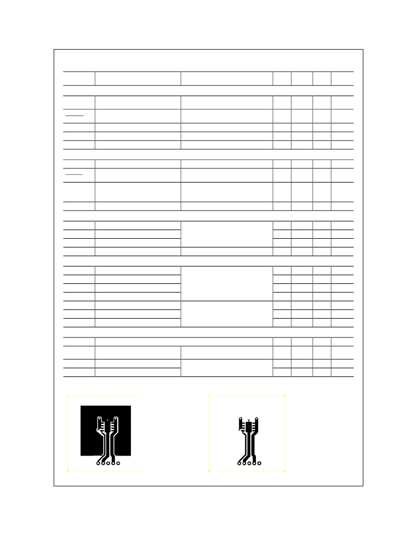
Scale 1 : 1 on letter size paper
2.
Pulse Test: Pulse Width < 300
μ
s, Duty Cycle < 2.0%
F
相關PDF資料 |
PDF描述 |
|---|---|
| FDS6294 | 30V N-Channel Fast Switching PowerTrench? MOSFET |
| FDS6298 | 30V N-Channel Fast Switching PowerTrench MOSFET |
| FDS6299S | 30V N-Channel PowerTrench SyncFET |
| FDS6375 | CONN RCPT .100 100POS DUAL HORZ |
| FDS6570A | Single N-Channel 2.5V Specified PowerTrench MOSFET |
相關代理商/技術參數 |
參數描述 |
|---|---|
| FDS6162N7 | 制造商:Fairchild Semiconductor Corporation 功能描述:MOSFET N CH 20V 23A 8SOIC |
| FDS6162N7 | 制造商:Fairchild Semiconductor Corporation 功能描述:MOSFET |
| FDS6294 | 功能描述:MOSFET 30V N-Ch PowerTrench Fast Switching RoHS:否 制造商:STMicroelectronics 晶體管極性:N-Channel 汲極/源極擊穿電壓:650 V 閘/源擊穿電壓:25 V 漏極連續電流:130 A 電阻汲極/源極 RDS(導通):0.014 Ohms 配置:Single 最大工作溫度: 安裝風格:Through Hole 封裝 / 箱體:Max247 封裝:Tube |
| FDS6294 | 制造商:Fairchild Semiconductor Corporation 功能描述:MOSFET |
| FDS6294_07 | 制造商:FAIRCHILD 制造商全稱:Fairchild Semiconductor 功能描述:30V N-Channel Fast Switching PowerTrench MOSFET |
發布緊急采購,3分鐘左右您將得到回復。