- 您現在的位置:買賣IC網 > PDF目錄375798 > FIN12ACMLX (FAIRCHILD SEMICONDUCTOR CORP) Low Voltage 12-Bit Bi-Directional Serializer/Deserializer with Multiple Frequency Ranges (Preliminary) PDF資料下載
參數資料
| 型號: | FIN12ACMLX |
| 廠商: | FAIRCHILD SEMICONDUCTOR CORP |
| 元件分類: | 通用總線功能 |
| 英文描述: | Low Voltage 12-Bit Bi-Directional Serializer/Deserializer with Multiple Frequency Ranges (Preliminary) |
| 中文描述: | LINE TRANSCEIVER, PQCC32 |
| 封裝: | 5 X 5 MM, LEAD FREE, MO-220WHHD-4, MLP-32 |
| 文件頁數: | 11/21頁 |
| 文件大小: | 1819K |
| 代理商: | FIN12ACMLX |
Preliminary
11
www.fairchildsemi.com
F
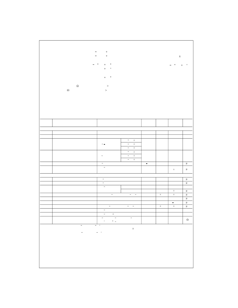
Absolute Maximum Ratings
(Note )
Recommended Operating
Conditions
Note 2:
Absolute maximum ratings are DC values beyond which the device
may be damaged or have its useful life impaired. The datasheet specifica-
tions should be met, without exception, to ensure that the system design is
reliable over its power supply, temperature, and output/input loading vari-
ables. Fairchild does not recommend operation outside datasheet specifi-
cations.
DC Electrical Characteristics
Over supply voltage and operating temperature ranges, unless otherwise specified.
Note 3:
Typical Values are given for V
DD
2.5V and T
A
25
q
C. Positive current values refer tot the current flowing into device and negative values means
current flowing out of pins. Voltage are referenced to Ground unless otherwise specified (except
'
V
OD
and V
OD
).
Note 4:
Typical values are given for V
DDP
2.75V and T
A
25
q
C.
Note 5:
The definition of short-circuit includes all the possible situations. For example, the short of differential pairs to Ground, the short of differential pairs
(No Grounding) and either line of differential pairs tied to Ground.
Supply Voltage (V
DD
)
ALL Input/Output Voltage
CTL Output Short Circuit Duration
Storage Temperature Range (T
STG
)
Maximum Junction Temperature (T
J
)
Lead Temperature (T
L
)
(Soldering, 4 seconds)
ESD Rating
Human Body Model, 1.5K
:
, 100pF
Machine Model, 0
:
, 200pF
0.5V to 4.6V
0.5V to 4.6V
Continuous
65
q
C to 150
q
C
150
q
C
260
q
C
!
2kV
!
200V
Supply Voltage (V
DDA
, V
DDS
)
Supply Voltage (V
DDP
)
Operating Temperature (T
A
) (Note )
Supply Noise Voltage (V
DDA-PP
)
2.775V
r
5.0%V
1.65V to 3.6V
10
q
C to 70
q
C
100 mV
P-P
Symbol
Parameter
Test Conditions
Min
Typ
(Note )
Max
Unit
LVCMOS I/O
V
IH
V
IL
V
OH
Input High Voltage
Input Low Voltage
0.65 x V
DDP
GND
V
DDP
0.35 x V
DDP
V
Output High Voltage
I
OH
2.0 mA
V
DDP
3.3
r
0.3
V
DDP
2.5
r
0.2
V
DDP
1.8
r
0.15
V
DDP
3.3
r
0.3
V
DDP
2.5
r
0.2
V
DDP
1.8
r
0.15
0.75 x V
DDP
V
V
OL
Output Low Voltage
V
I
OL
2.0 mA
0.25 x V
DDP
I
IN
I
OFF
Input Current
Input/Output Power-Off
Leakage Current
V
IN
0V to 3.6V
V
DDP
0V,
ALL LVCMOS Inputs/ Outputs 0V to 3.6V
5.0
5.0
P
A
r
5.0
P
A
DIFFERENTIAL I/O
(Note )
I
ODH
Output HIGH Source Current
I
ODL
Output LOW Sink Current
I
OS
Short Circuit Output Current
V
OS
1.0V Figure
V
OS
1.0V Figure
V
OUT
0V
TBD
TBD
P
A
P
A
Driver Enabled
Driver Disabled
mA
P
A
P
A
r
5.0
r
5.0
I
OZ
I
TH
I
TL
I
IZ
I
IS
V
ICM
R
TRM
Disabled Output Leakage Current
CKSO, DSO
0V to V
DDS
, S2
S1
0V
r
1.0
Differential Input Threshold HIGH Current See Figure and Table
Differential Input Threshold LOW Current
Disabled Input Leakage Current
50.0
P
A
P
A
P
A
See Figure and Table
CKSI, DSI
0V to V
DDS
, S2
S1
0V
V
OUT
V
DDS
V
DDS
2.775
r
5%
V
ID
50mV, V
IC
925mV, DIR I
0
|CKSI
- CKSI
|
V
ID
50.0
r
5.0
r
1.0
Short Circuit Input Current
Input Common Mode Range
CKSI, DS Internal Receiver
mA
V
0.5
V
DDS-1
100
:
Termination Resistor
相關PDF資料 |
PDF描述 |
|---|---|
| FIN1531M | 5V LVDS 4-Bit High Speed Differential Driver |
| FIN1531MTC | 5V LVDS 4-Bit High Speed Differential Driver |
| FIN1531MTCX | LINE DRIVER|4 DRIVER|CMOS|TSSOP|16PIN|PLASTIC |
| FIN1531MX | LINE DRIVER|4 DRIVER|CMOS|SOP|16PIN|PLASTIC |
| FIN1531 | 5V LVDS 4-Bit High Speed Differential Driver |
相關代理商/技術參數 |
參數描述 |
|---|---|
| FIN12Y WAF | 制造商:Fairchild Semiconductor Corporation 功能描述: |
| FIN1531 | 制造商:FAIRCHILD 制造商全稱:Fairchild Semiconductor 功能描述:5V LVDS 4-Bit High Speed Differential Driver |
| FIN1531M | 功能描述:LVDS 接口集成電路 5V Hi Speed Driver LVDS 4Bit Differ RoHS:否 制造商:Texas Instruments 激勵器數量:4 接收機數量:4 數據速率:155.5 Mbps 工作電源電壓:5 V 最大功率耗散:1025 mW 最大工作溫度:+ 85 C 封裝 / 箱體:SOIC-16 Narrow 封裝:Reel |
| FIN1531M_Q | 功能描述:LVDS 接口集成電路 5V Hi Speed Driver LVDS 4Bit Differ RoHS:否 制造商:Texas Instruments 激勵器數量:4 接收機數量:4 數據速率:155.5 Mbps 工作電源電壓:5 V 最大功率耗散:1025 mW 最大工作溫度:+ 85 C 封裝 / 箱體:SOIC-16 Narrow 封裝:Reel |
| FIN1531MTC | 功能描述:LVDS 接口集成電路 5V Hi Speed Driver LVDS 4Bit Differ RoHS:否 制造商:Texas Instruments 激勵器數量:4 接收機數量:4 數據速率:155.5 Mbps 工作電源電壓:5 V 最大功率耗散:1025 mW 最大工作溫度:+ 85 C 封裝 / 箱體:SOIC-16 Narrow 封裝:Reel |
發布緊急采購,3分鐘左右您將得到回復。