- 您現在的位置:買賣IC網 > PDF目錄375884 > FQI20N06L (FAIRCHILD SEMICONDUCTOR CORP) 60V LOGIC N-Channel MOSFET PDF資料下載
參數資料
| 型號: | FQI20N06L |
| 廠商: | FAIRCHILD SEMICONDUCTOR CORP |
| 元件分類: | JFETs |
| 英文描述: | 60V LOGIC N-Channel MOSFET |
| 中文描述: | 21 A, 60 V, 0.07 ohm, N-CHANNEL, Si, POWER, MOSFET, TO-262 |
| 封裝: | I2PAK-3 |
| 文件頁數: | 2/9頁 |
| 文件大小: | 680K |
| 代理商: | FQI20N06L |
F
Rev. A1. May 2001
2001 Fairchild Semiconductor Corporation
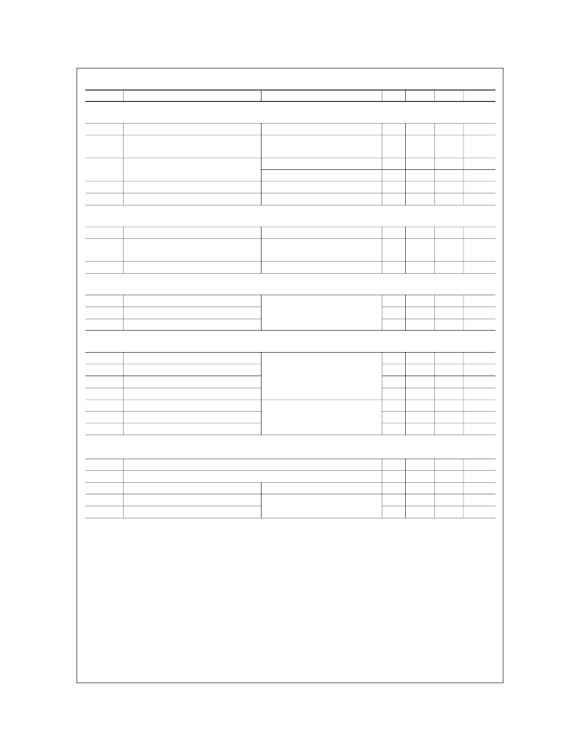
Electrical Characteristics
T
C
= 25°C unless otherwise noted
Notes:
1. Repetitive Rating : Pulse width limited by maximum junction temperature
2. L = 450
μ
H, I
= 21A, V
DD
= 25V, R
= 25
,
Starting T
= 25°C
3. I
≤
21A, di/dt
≤
300A/
μ
s, V
DD
≤
BV
Starting T
J
= 25°C
4. Pulse Test : Pulse width
≤
300
μ
s, Duty cycle
≤
2%
5. Essentially independent of operating temperature
Symbol
Parameter
Test Conditions
Min
Typ
Max
Units
Off Characteristics
BV
DSS
Drain-Source Breakdown Voltage
BV
DSS
/
T
J
Coefficient
I
DSS
Zero Gate Voltage Drain Current
V
GS
= 0 V, I
D
= 250
μ
A
60
--
--
V
Breakdown Voltage Temperature
I
D
= 250
μ
A, Referenced to 25°C
--
0.06
--
V/°C
V
DS
= 60 V, V
GS
= 0 V
V
DS
= 48 V, T
C
= 150°C
V
GS
= 20 V, V
DS
= 0 V
V
GS
= -20 V, V
DS
= 0 V
--
--
--
--
--
--
--
--
1
10
100
-100
μ
A
μ
A
nA
nA
I
GSSF
I
GSSR
Gate-Body Leakage Current, Forward
Gate-Body Leakage Current, Reverse
On Characteristics
V
GS(th)
Gate Threshold Voltage
R
DS(on)
Static Drain-Source
On-Resistance
g
FS
Forward Transconductance
V
DS
= V
GS
, I
D
= 250
μ
A
V
GS
= 10 V, I
D
= 10.5 A
V
GS
= 5 V, I
D
=10.5 A
V
DS
= 25 V, I
D
= 10.5 A
1.0
--
--
--
--
2.5
0.055
0.07
--
V
0.042
0.055
11
S
Dynamic Characteristics
C
iss
Input Capacitance
C
oss
Output Capacitance
C
rss
Reverse Transfer Capacitance
V
DS
= 25 V, V
GS
= 0 V,
f = 1.0 MHz
--
--
--
480
175
35
630
230
45
pF
pF
pF
Switching Characteristics
t
d(on)
Turn-On Delay Time
t
r
Turn-On Rise Time
t
d(off)
Turn-Off Delay Time
t
f
Turn-Off Fall Time
Q
g
Total Gate Charge
Q
gs
Gate-Source Charge
Q
gd
Gate-Drain Charge
V
DD
= 30 V, I
D
= 10.5 A,
R
G
= 25
--
--
--
--
--
--
--
10
165
35
70
9.5
2.5
5.5
30
340
80
150
13
--
--
ns
ns
ns
ns
nC
nC
nC
V
DS
= 48 V, I
D
= 21 A,
V
GS
= 5 V
Drain-Source Diode Characteristics and Maximum Ratings
I
S
Maximum Continuous Drain-Source Diode Forward Current
I
SM
Maximum Pulsed Drain-Source Diode Forward Current
V
SD
Drain-Source Diode Forward Voltage
t
rr
Reverse Recovery Time
Q
rr
Reverse Recovery Charge
--
--
--
--
--
--
--
--
54
75
21
84
1.5
--
--
A
A
V
ns
nC
V
GS
= 0 V, I
S
= 21 A
V
GS
= 0 V, I
S
= 21 A,
dI
F
/ dt = 100 A/
μ
s
(Note 4)
(Note 4, 5)
(Note 4, 5)
(Note 4)
相關PDF資料 |
PDF描述 |
|---|---|
| FQB20N06L | 60V LOGIC N-Channel MOSFET |
| FQI20N06 | 60V N-Channel MOSFET |
| FQB20N06 | 60V N-Channel MOSFET |
| FQI24N08 | 80V N-Channel MOSFET |
| FQB24N08 | 80V N-Channel MOSFET |
相關代理商/技術參數 |
參數描述 |
|---|---|
| FQI22N30 | 制造商:未知廠家 制造商全稱:未知廠家 功能描述:TRANSISTOR | MOSFET | N-CHANNEL | 300V V(BR)DSS | 21A I(D) | TO-263 |
| FQI22N30TU | 功能描述:MOSFET DISC BY MFG 2/02 RoHS:否 制造商:STMicroelectronics 晶體管極性:N-Channel 汲極/源極擊穿電壓:650 V 閘/源擊穿電壓:25 V 漏極連續電流:130 A 電阻汲極/源極 RDS(導通):0.014 Ohms 配置:Single 最大工作溫度: 安裝風格:Through Hole 封裝 / 箱體:Max247 封裝:Tube |
| FQI22P10 | 制造商:FAIRCHILD 制造商全稱:Fairchild Semiconductor 功能描述:100V P-Channel MOSFET |
| FQI24N08 | 制造商:FAIRCHILD 制造商全稱:Fairchild Semiconductor 功能描述:80V N-Channel MOSFET |
| FQI26N03L | 制造商:未知廠家 制造商全稱:未知廠家 功能描述:TRANSISTOR | MOSFET | N-CHANNEL | 30V V(BR)DSS | 26A I(D) | TO-263 |
發布緊急采購,3分鐘左右您將得到回復。