- 您現(xiàn)在的位置:買賣IC網 > PDF目錄371036 > MC44724 (Motorola, Inc.) Digital Video Encoder PDF資料下載
參數(shù)資料
| 型號: | MC44724 |
| 廠商: | Motorola, Inc. |
| 英文描述: | Digital Video Encoder |
| 中文描述: | 數(shù)字視頻編碼器 |
| 文件頁數(shù): | 4/39頁 |
| 文件大小: | 518K |
| 代理商: | MC44724 |
第1頁第2頁第3頁當前第4頁第5頁第6頁第7頁第8頁第9頁第10頁第11頁第12頁第13頁第14頁第15頁第16頁第17頁第18頁第19頁第20頁第21頁第22頁第23頁第24頁第25頁第26頁第27頁第28頁第29頁第30頁第31頁第32頁第33頁第34頁第35頁第36頁第37頁第38頁第39頁
MC44724/5 Rev 0.21 03/25/97
No.
This document contains information on a new product. Specifications and information herein are subject to change without notice.
4
I2C/SPI chip-address 40/41(hex)
1D/1E(hex)
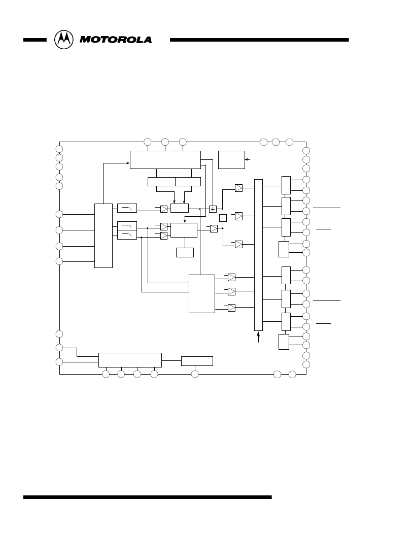
[Block Diagram]
D
Y/G1
Y/G1
C/Cr/R1
C/Cr/R1
CVBS/Cb/B1
CVBS/Cb/B1
Y/G1Vdd
CVBS/Cb/B1Vdd
C/Cr/R1Vdd
E
F
H
DVIN [7 : 0]
0
0
0
0
CGMS,
WSS_gen
CC_gen
Sync_generator
copy
protection
bus
off_set
BG
Modulator
subcarrier
gen
0
D
0
D
0
TVIN
demux
Y
Cb
Cr
H,V
ChipA
DVdd
DVdd
DVss
DVss
MC44724/5
DAVdd
DAVss
Ibias1
B
Vref1
S
S
T
TEST
PAL/NTSC
Reset
clock
S
S
I2C / SPI
RGB matrix
0
0
0
D
Y/G2
Y/G2
C/Cr/R2
C/Cr/R2
CVBS/Cb/B2
CVBS/Cb/B2
D
D
Ibias2
B
Vref2
TP [8 : 1]
D
D
Y
C
C
O
bus
TP [0]
發(fā)布緊急采購,3分鐘左右您將得到回復。