- 您現在的位置:買賣IC網 > PDF目錄371051 > MC68HC11KA4TS (Motorola, Inc.) KPT 3C 3#16 PIN PLUG PDF資料下載
參數資料
| 型號: | MC68HC11KA4TS |
| 廠商: | Motorola, Inc. |
| 英文描述: | KPT 3C 3#16 PIN PLUG |
| 中文描述: | 8位微控制器 |
| 文件頁數: | 33/68頁 |
| 文件大小: | 365K |
| 代理商: | MC68HC11KA4TS |
第1頁第2頁第3頁第4頁第5頁第6頁第7頁第8頁第9頁第10頁第11頁第12頁第13頁第14頁第15頁第16頁第17頁第18頁第19頁第20頁第21頁第22頁第23頁第24頁第25頁第26頁第27頁第28頁第29頁第30頁第31頁第32頁當前第33頁第34頁第35頁第36頁第37頁第38頁第39頁第40頁第41頁第42頁第43頁第44頁第45頁第46頁第47頁第48頁第49頁第50頁第51頁第52頁第53頁第54頁第55頁第56頁第57頁第58頁第59頁第60頁第61頁第62頁第63頁第64頁第65頁第66頁第67頁第68頁
MC68HC11KA4
MC68HC11KA4TS/D
MOTOROLA
33
DDA[7:0] —Data Direction for Port A
0 = Bits set to zero to configure corresponding I/O pin for input only
1 = Bits set to one to configure corresponding I/O pin for output
Reset state is mode dependent. In single-chip or bootstrap modes, port B pins are high impedance in-
puts with selectable internal pull-up resistors. In expanded or test modes, port B pins are high order ad-
dress outputs and PORTB is not in the memory map.
DDB[7:0] — Data Direction for Port B
0 = Bits set to zero to configure corresponding I/O pin for input only
1 = Bits set to one to configure corresponding I/O pin for output
Reset state is mode dependent. In single-chip or bootstrap modes, port F pins are high-impedance in-
puts with selectable internal pull-up resistors. In expanded or test modes, port F pins are low order ad-
dress outputs and PORTF is not in the memory map.
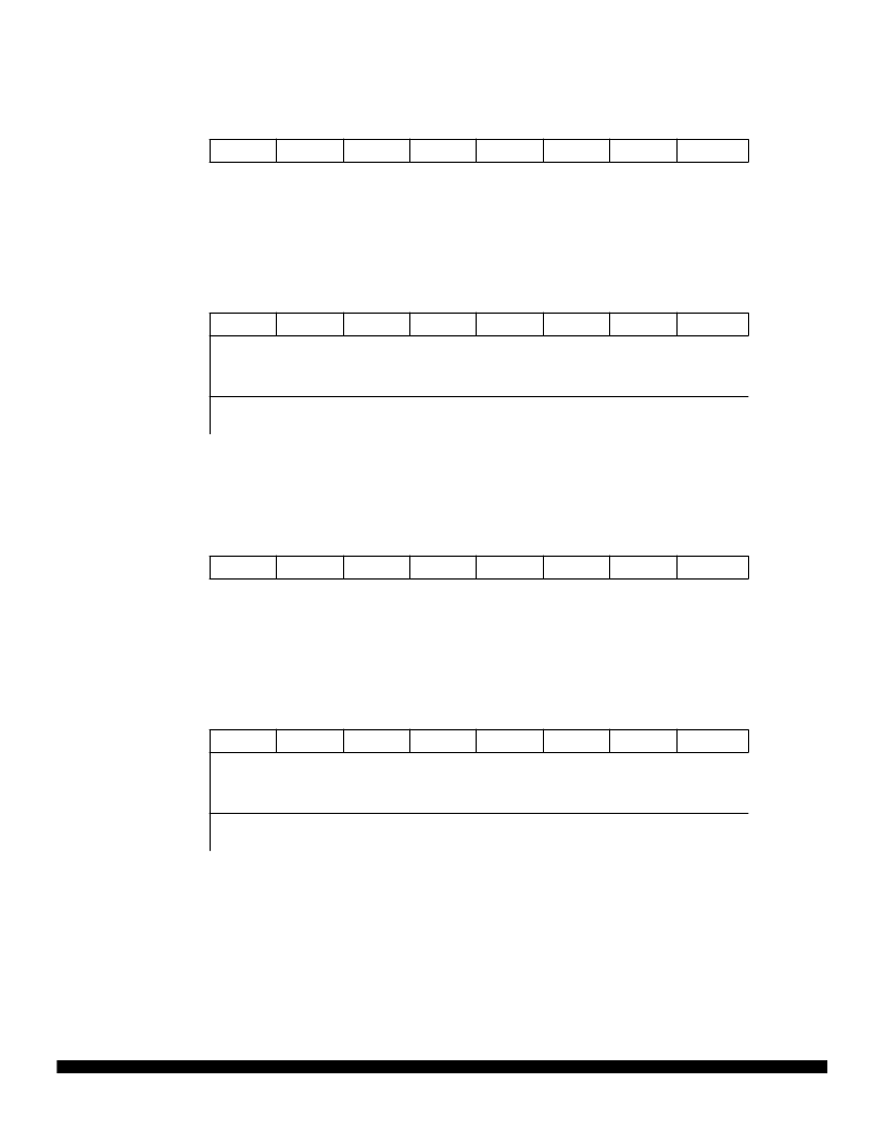
DDRA
— Data Direction Register for Port A
$0001
Bit 7
6
5
4
3
2
1
Bit 0
DDA7
DDA6
DDA5
DDA4
DDA3
DDA2
DDA1
DDA0
RESET:
0
0
0
0
0
0
0
0
PORTB
—Port B Data
$0004
Bit 7
6
5
4
3
2
1
Bit 0
PB7
PB6
PB5
PB4
PB3
PB2
PB1
PB0
S. Chip or
Boot:
PB7
PB6
PB5
PB4
PB3
PB2
PB1
PB0
RESET:
U
U
U
U
U
U
U
U
Expan. or
Test:
ADDR15
ADDR14
ADDR13
ADDR12
ADDR11
ADDR10
ADDR9
ADDR8
DDRB
— Data Direction Register for Port B
$0002
Bit 7
6
5
4
3
2
1
Bit 0
DDB7
DDB6
DDB5
DDB4
DDB3
DDB2
DDB1
DDB0
RESET:
0
0
0
0
0
0
0
0
PORTF
— Port F Data
$0005
Bit 7
6
5
4
3
2
1
Bit 0
PF7
PF6
PF5
PF4
PF3
PF2
PF1
PF0
S. Chip or
Boot:
PF7
PF6
PF5
PF4
PF3
PF2
PF1
PF0
RESET:
U
U
U
U
U
U
U
U
Expan. or
Test:
ADDR7
ADDR6
ADDR5
ADDR4
ADDR3
ADDR2
ADDR1
ADDR0
相關PDF資料 |
PDF描述 |
|---|---|
| MC68HC11KW1 | High-density complementary metal oxide semiconductor HCMOS) microcontroller unit |
| MC68HC11L6CFN | HCMOS MICROCONTROLLER UNIT |
| MC68HC11L6FS | HCMOS MICROCONTROLLER UNIT |
| MC68HC11L6FU | HCMOS MICROCONTROLLER UNIT |
| MC68HC11L6L | HCMOS MICROCONTROLLER UNIT |
相關代理商/技術參數 |
參數描述 |
|---|---|
| MC68HC11KA4VFN2 | 制造商:未知廠家 制造商全稱:未知廠家 功能描述:8-Bit Microcontroller |
| MC68HC11KA4VFN3 | 制造商:未知廠家 制造商全稱:未知廠家 功能描述:8-Bit Microcontroller |
| MC68HC11KA4VFN4 | 制造商:未知廠家 制造商全稱:未知廠家 功能描述:8-Bit Microcontroller |
| MC68HC11KA4VFU2 | 制造商:未知廠家 制造商全稱:未知廠家 功能描述:8-Bit Microcontroller |
| MC68HC11KA4VFU3 | 制造商:未知廠家 制造商全稱:未知廠家 功能描述:8-Bit Microcontroller |
發(fā)布緊急采購,3分鐘左右您將得到回復。