- 您現在的位置:買賣IC網 > PDF目錄371055 > MC74ACT350N (MOTOROLA INC) 4-BIT SHIFTER WITH 3-STATE OUTPUTS PDF資料下載
MC74AC350 MC74ACT350
5-4
FACT DATA
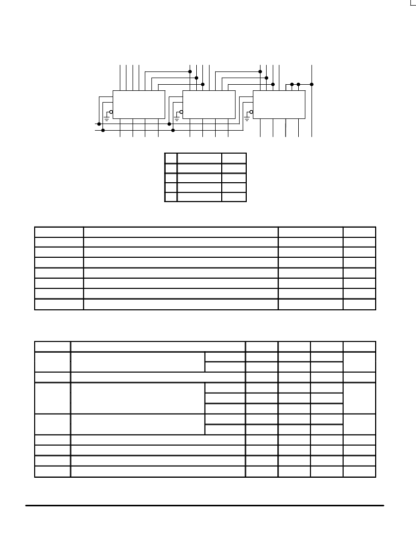
13-Bit Twos Complement Scaler
S0
S1
OE
Y0
Y1
Y2
Y3
I–3
I–1I0
I1
I2
I3
I–2
S0
S1
OE
Y0
Y1
Y2
Y3
I–3
I–1I0
I1
I2
I3
I–2
S0
S1
OE
Y0
Y1
Y2
Y3
I–3
I–1I0
I1
I2
I3
I–2
12 11 10 9
12
11
10
9
8 7 6 5
4 3 2 1
S
8
7
6
5
4
3
2
1
S
S0
S1
S1
L
S0
L
÷
8
H
÷
4
L
÷
2
SCALE
1/8
L
1/4
H
1/2
H
H NO CHANGE
1
MAXIMUM RATINGS*
Symbol
Parameter
Value
Unit
VCC
Vin
Vout
Iin
Iout
ICC
Tstg
DC Supply Voltage (Referenced to GND)
–0.5 to +7.0
V
DC Input Voltage (Referenced to GND)
–0.5 to VCC +0.5
–0.5 to VCC +0.5
±
20
V
DC Output Voltage (Referenced to GND)
V
DC Input Current, per Pin
mA
DC Output Sink/Source Current, per Pin
±
50
mA
DC VCC or GND Current per Output Pin
Storage Temperature
±
50
mA
–65 to +150
°
C
* Maximum Ratings are those values beyond which damage to the device may occur. Functional operation should be restricted to the Recommended
Operating Conditions.
RECOMMENDED OPERATING CONDITIONS
Symbol
Parameter
Min
Typ
Max
Unit
VCC
Supply Voltage
′
AC
′
ACT
2.0
5.0
6.0
V
4.5
5.0
5.5
Vin, Vout
DC Input Voltage, Output Voltage (Ref. to GND)
0
VCC
V
′
AC Devices except Schmitt Inputs
VCC @ 3.0 V
VCC @ 4.5 V
VCC @ 5.5 V
VCC @ 4.5 V
150
tr, tf
Input Rise and Fall Time (Note 1)
40
ns/V
25
tr, tf
Input Rise and Fall Time (Note 2)
′
ACT Devices except Schmitt Inputs
10
ns/V
VCC @ 5.5 V
8.0
TJ
TA
IOH
IOL
Junction Temperature (PDIP)
140
°
C
Operating Ambient Temperature Range
–40
25
85
°
C
Output Current — High
–24
mA
Output Current — Low
24
mA
1. Vin from 30% to 70% VCC; see individual Data Sheets for devices that differ from the typical input rise and fall times.
2. Vin from 0.8 V to 2.0 V; see individual Data Sheets for devices that differ from the typical input rise and fall times.
相關PDF資料 |
PDF描述 |
|---|---|
| MC74AC350N | 4-BIT SHIFTER WITH 3-STATE OUTPUTS |
| MC74AC352D | DUAL 4-INPUT MULTIPLEXER |
| MC74ACT352 | DUAL 4-INPUT MULTIPLEXER |
| MC74AC352 | DUAL 4-INPUT MULTIPLEXER |
| MC74ACT352D | DUAL 4-INPUT MULTIPLEXER |
相關代理商/技術參數 |
參數描述 |
|---|---|
| MC74ACT352 | 制造商:MOTOROLA 制造商全稱:Motorola, Inc 功能描述:DUAL 4-INPUT MULTIPLEXER |
| MC74ACT352D | 制造商:MOTOROLA 制造商全稱:Motorola, Inc 功能描述:DUAL 4-INPUT MULTIPLEXER |
| MC74ACT352N | 制造商:MOTOROLA 制造商全稱:Motorola, Inc 功能描述:DUAL 4-INPUT MULTIPLEXER |
| MC74ACT353 | 制造商:MOTOROLA 制造商全稱:Motorola, Inc 功能描述:DUAL 4-INPUT MULTIPLEXER WITH 3-STATE OUTPUTS |
| MC74ACT353D | 制造商:Rochester Electronics LLC 功能描述:- Bulk 制造商:ON Semiconductor 功能描述: |
發布緊急采購,3分鐘左右您將得到回復。