- 您現在的位置:買賣IC網 > PDF目錄371036 > MC74HC254A (Motorola, Inc.) Octal 3-State Noninverting Buffer Transceiver PDF資料下載
參數資料
| 型號: | MC74HC254A |
| 廠商: | Motorola, Inc. |
| 英文描述: | Octal 3-State Noninverting Buffer Transceiver |
| 中文描述: | 八路三態收發器同相緩沖 |
| 文件頁數: | 3/7頁 |
| 文件大小: | 149K |
| 代理商: | MC74HC254A |
MC54/74HC245A
High–Speed CMOS Logic Data
DL129 — Rev 6
3
MOTOROLA
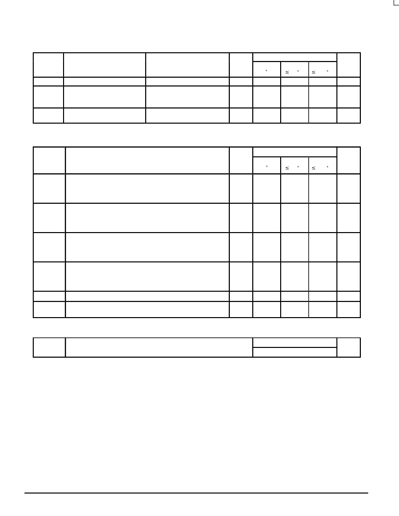
(Voltages Referenced to GND)
μ
A
±
0.5
±
5.0
25 C
±
0.1
6.0
Output in High–Impedance State
Vin = VIL or VIH
Vout = VCC or GND
Vin = VCC or GND
Maximum Three–State Leakage
Current
IOZ
Unit
μ
A
±
10
125 C
±
1.0
85 C
±
1.0
V
Test Conditions
Vin = VCC or GND
Parameter
Symbol
Iin
NOTE:Information on typical parametric values and high frequency or heavy load considerations can be found in Chapter 2 of the Motorola High–
Speed CMOS Data Book (DL129/D).
AC ELECTRICAL CHARACTERISTICS
(CL = 50 pF, Input tr = tf = 6 ns)
ICC
Maximum Input Leakage Current
6.0
4.0
40
Maximum Quiescent Supply
6.0
160
μ
A
b l
V
15
Guaranteed Limit
Speed CMOS Data Book (DL129/D).
– 55 to
6.0
Maximum Propagation Delay, A to B, B to A
(Figures 1 and 3)
4.5
22
22
19
22
Maximum Propagation Delay, Direction or Output Enable to A or B
(Figures 2 and 4)
4.5
23
12
28
33
Maximum Propagation Delay, Output Enable to A or B
(Figures 2 and 4)
4.5
28
33
Maximum Output Transition Time, Any Output
(Figures 1 and 3)
4.5
15
18
(I/O in High–Impedance State)
Maximum Three–State I/O Capacitance
CPD
Power Dissipation Capacitance (Per Transceiver Channel)*
* Used to determine the no–load dynamic power consumption: PD = CPD VCC2f + ICC VCC. For load considerations, see Chapter 2 of the
Motorola High–Speed CMOS Data Book (DL129/D).
Typical @ 25
°
C, VCC = 5.0 V
40
pF
相關PDF資料 |
PDF描述 |
|---|---|
| MC54-74HC259A | 8-Bit Addressable Latch 1-of-8 Decoder |
| MC74HC259A | 8-Bit Addressable Latch 1-of-8 Decoder |
| MC74HC259AD | 8-Bit Addressable Latch 1-of-8 Decoder |
| MC74HC259ADT | 8-Bit Addressable Latch 1-of-8 Decoder |
| MC74HC259AN | 8-Bit Addressable Latch 1-of-8 Decoder |
相關代理商/技術參數 |
參數描述 |
|---|---|
| MC74HC257D | 制造商:Motorola Inc 功能描述: |
| MC74HC257DR2 | 制造商:Motorola 功能描述:74HC257 |
| MC74HC257FR2 | 制造商:Rochester Electronics LLC 功能描述:- Bulk |
| MC74HC257N | 制造商:Motorola Inc 功能描述: |
| MC74HC257ND | 制造商:Motorola Inc 功能描述: |
發布緊急采購,3分鐘左右您將得到回復。