- 您現在的位置:買賣IC網 > PDF目錄98228 > THS7303PW (TEXAS INSTRUMENTS INC) 3 CHANNEL, VIDEO AMPLIFIER, PDSO20 PDF資料下載
參數資料
| 型號: | THS7303PW |
| 廠商: | TEXAS INSTRUMENTS INC |
| 元件分類: | 音頻/視頻放大 |
| 英文描述: | 3 CHANNEL, VIDEO AMPLIFIER, PDSO20 |
| 封裝: | GREEN, PLASTIC, TSSOP-20 |
| 文件頁數: | 40/60頁 |
| 文件大小: | 1980K |
| 代理商: | THS7303PW |
第1頁第2頁第3頁第4頁第5頁第6頁第7頁第8頁第9頁第10頁第11頁第12頁第13頁第14頁第15頁第16頁第17頁第18頁第19頁第20頁第21頁第22頁第23頁第24頁第25頁第26頁第27頁第28頁第29頁第30頁第31頁第32頁第33頁第34頁第35頁第36頁第37頁第38頁第39頁當前第40頁第41頁第42頁第43頁第44頁第45頁第46頁第47頁第48頁第49頁第50頁第51頁第52頁第53頁第54頁第55頁第56頁第57頁第58頁第59頁第60頁
SLOS479B
– OCTOBER 2005 – REVISED MARCH 2011
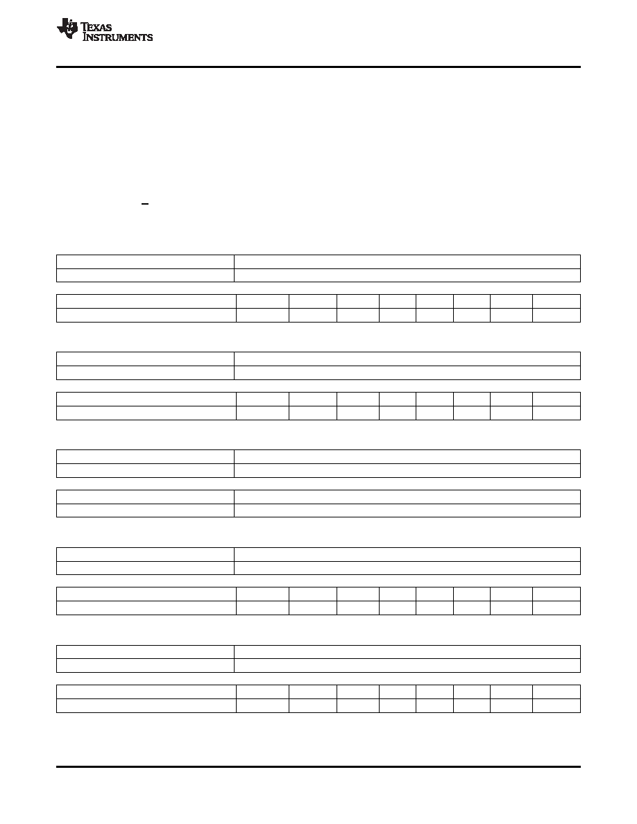
EXAMPLE: READING FROM THE THS7303
The read operation consists of two phases. The first phase is the address phase, where an I2C master initiates a
write operation to the THS7303 by generating a start condition (S) followed by the THS7303 I2C address in MSB
first bit order, followed by a '0' to indicate a write cycle. After receiving acknowledges from the THS7303, the
master presents the sub-address (channel) of the register it wants to read. After the cycle is acknowledged (A),
the master terminates the cycle immediately by generating a stop condition (P).
The second phase is the data phase. In this phase, an I2C master initiates a read operation to the THS7303 by
generating a start condition followed by the THS7303 I2C address in MSB first bit order, followed by a '1' to
indicate a read cycle. After an acknowledge from the THS7303, the I2C master receives one byte of data from
the THS7303. After the data byte has been transferred from the THS7303 to the master, the master generates a
not acknowledge (A) followed by a stop. As with the write function, in order to read all channels, steps 1 through
11 must be repeated for each channel desired.
Example of THS7303 Read Phase 1:
Step 1
0
I2C Start (Master)
S
Step 2
7
6
5
4
3
2
1
0
I2C General Address (Master)
0
1
0
1
X
0
Where each X logic state is defined by I2C A1 and I2C A0 pins being tied to either VS+ or GND.
Step 3
9
I2C Acknowledge (Slave)
A
Step 4
7
6
5
4
3
2
1
0
I2C Read Channel Address (Master)
0
Addr
Where Addr is determined by the values shown in Table 2.
Step 5
9
I2C Acknowledge (Slave)
A
Step 6
0
I2C Start (Master)
P
Example of THS7303 Read Phase 2:
Step 7
0
I2C Start (Master)
S
Step 8
7
6
5
4
3
2
1
0
I2C General Address (Master)
0
1
0
1
X
1
Where each X logic state is defined by I2C A1 and I2C A0 pins being tied to either VS+ or GND.
Step 9
9
I2C Acknowledge (Slave)
A
Step 10
7
6
5
4
3
2
1
0
I2C Read Data (Slave)
Data
Copyright
2005–2011, Texas Instruments Incorporated
45
Product Folder Link(s): THS7303
相關PDF資料 |
PDF描述 |
|---|---|
| THS7303PWG4 | 3 CHANNEL, VIDEO AMPLIFIER, PDSO20 |
| THS7303PWRG4 | 3 CHANNEL, VIDEO AMPLIFIER, PDSO20 |
| THS7315DR | 3 CHANNEL, VIDEO AMPLIFIER, PDSO8 |
| THS7315D | 3 CHANNEL, VIDEO AMPLIFIER, PDSO8 |
| THS7315DG4 | 3 CHANNEL, VIDEO AMPLIFIER, PDSO8 |
相關代理商/技術參數 |
參數描述 |
|---|---|
| THS7303PWG4 | 功能描述:視頻放大器 3-Ch Low Power Video RoHS:否 制造商:ON Semiconductor 通道數量:4 電源類型: 工作電源電壓:3.3 V, 5 V 電源電流: 最小工作溫度: 最大工作溫度: 封裝 / 箱體:TSSOP-14 封裝:Reel |
| THS7303PWR | 功能描述:視頻放大器 3-Ch Low Power Video RoHS:否 制造商:ON Semiconductor 通道數量:4 電源類型: 工作電源電壓:3.3 V, 5 V 電源電流: 最小工作溫度: 最大工作溫度: 封裝 / 箱體:TSSOP-14 封裝:Reel |
| THS7303PWRG4 | 功能描述:視頻放大器 3-Ch Low Power Video RoHS:否 制造商:ON Semiconductor 通道數量:4 電源類型: 工作電源電壓:3.3 V, 5 V 電源電流: 最小工作溫度: 最大工作溫度: 封裝 / 箱體:TSSOP-14 封裝:Reel |
| THS730A A2 | 制造商:Tektronix Inc 功能描述:OSCILLOSCOPE DSO/DMM 200MHZ |
發布緊急采購,3分鐘左右您將得到回復。