- 您現(xiàn)在的位置:買賣IC網(wǎng) > PDF目錄98229 > THS8083APZPG4 (TEXAS INSTRUMENTS INC) SPECIALTY CONSUMER CIRCUIT, PQFP100 PDF資料下載
參數(shù)資料
| 型號: | THS8083APZPG4 |
| 廠商: | TEXAS INSTRUMENTS INC |
| 元件分類: | 消費家電 |
| 英文描述: | SPECIALTY CONSUMER CIRCUIT, PQFP100 |
| 封裝: | GREEN, PLASTIC, HTQFP-100 |
| 文件頁數(shù): | 41/63頁 |
| 文件大小: | 320K |
| 代理商: | THS8083APZPG4 |
第1頁第2頁第3頁第4頁第5頁第6頁第7頁第8頁第9頁第10頁第11頁第12頁第13頁第14頁第15頁第16頁第17頁第18頁第19頁第20頁第21頁第22頁第23頁第24頁第25頁第26頁第27頁第28頁第29頁第30頁第31頁第32頁第33頁第34頁第35頁第36頁第37頁第38頁第39頁第40頁當(dāng)前第41頁第42頁第43頁第44頁第45頁第46頁第47頁第48頁第49頁第50頁第51頁第52頁第53頁第54頁第55頁第56頁第57頁第58頁第59頁第60頁第61頁第62頁第63頁
63
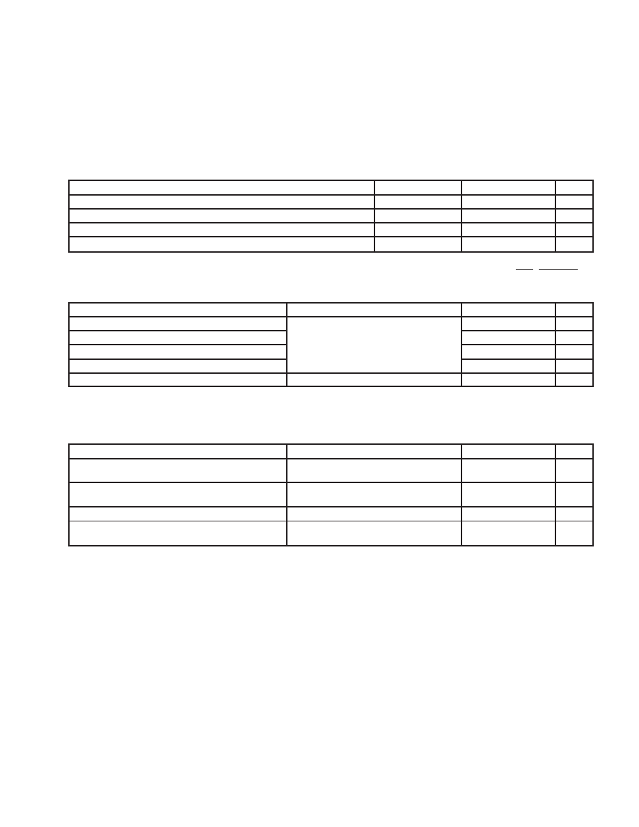
6.4
Electrical Characteristics Over Recommended Operating Free-Air Temperature
Range, TA = 0°C to 70°C (unless otherwise noted)
NOTE: In order to reach stated performance levels, the device’s PowerPad feature should be
thermally and electrically connected to the pcb ground plane, as described in Section 6.1
Designing With PowerPad.
6.4.1
Power Supply (3.3 V All Supplies)
PARAMETER
TEST CONDITIONS
MIN
TYP
MAX
UNIT
Analog supply (=AVDD_CH1+AVDD_CH2_3+AVDD_PLL+AVDD_REF)
ADC_INTREF
325
385
mA
Analog supply (=AVDD_CH1+AVDD_CH2_3+AVDD_PLL+AVDD_REF)
ADC_INTREF
325
385
mA
Digital supply (=DVDD+DVDD_PLL)
ADC_INTREF
119
140
mA
Digital supply (=DVDD+DVDD_PLL)
ADC_INTREF
119
140
mA
Total power dissipation normal operation
ADC_INTREF
1.47
1.73
W
Total power dissipation normal operation
ADC_INTREF
1.47
1.73
W
Total power dissipation, power down all modes
ADC_PWDN
385
mW
Total power dissipation, power down all modes
ADC_PWDN
385
mW
6.4.2
Digital Logic Inputs (HS, VS, SCL, SDA, I2CA, XTL1_MCLK, EXT_ADCCLK, OE, RESET,
EXT_CLP)
PARAMETER
TEST CONDITIONS
MIN
TYP
MAX
UNIT
IIH
High-level input current
10
A
IIL
Low-level input current
DVDD = 3.6 V,
Digital inputs and CLK at 0 V for IIL;
10
A
IIL(CLK)
Low-level input current, CLK (see Note 6)
Digital inputs and CLK at 0 V for IIL;
Digital inputs and CLK at 3.6 V for IIH
14
17
A
IIH(CLK) High-level input current , CLK (see Note 6)
Digital inputs and CLK at 3.6 V for IIH
14
17
A
CI
Input capacitance
5
pF
NOTE 6: Applies when XTL1_MCLK is driven by the clock signal directly.
6.4.3
Logic Outputs (SDA, CHn_OUTA[7..0], CHn_OUTB[7..0], DTOCLK3, ADCCLK2,
DATACLK1, DHS, LOCK)
PARAMETER
TEST CONDITIONS
MIN
TYP
MAX
UNIT
VOH
High-level output voltage
DVDD = 3 V at IOH = 50 A,
Digital output forced high
2.9
V
VOL
Low-level output voltage
DVDD = 3.6 V at IOL = 50 A,
Digital output forced low
0.15
V
CO
Output capacitance
5
pF
IOZ(H)/IOZ(L)
High-impedance-state output current
DVDD = 3.6 V
Worst case for VO = 3.6 V and VO = 0 V
10
A
Tested for CHn-A[7..0] and CHn_B[7..0] only
發(fā)布緊急采購,3分鐘左右您將得到回復(fù)。