- 您現(xiàn)在的位置:買(mǎi)賣(mài)IC網(wǎng) > PDF目錄98244 > TLC7524EFN (TEXAS INSTRUMENTS INC) PARALLEL, 8 BITS INPUT LOADING, 0.1 us SETTLING TIME, 8-BIT DAC, PQCC20 PDF資料下載
參數(shù)資料
| 型號(hào): | TLC7524EFN |
| 廠商: | TEXAS INSTRUMENTS INC |
| 元件分類(lèi): | DAC |
| 英文描述: | PARALLEL, 8 BITS INPUT LOADING, 0.1 us SETTLING TIME, 8-BIT DAC, PQCC20 |
| 封裝: | PLASTIC, LCC-20 |
| 文件頁(yè)數(shù): | 15/20頁(yè) |
| 文件大小: | 488K |
| 代理商: | TLC7524EFN |
第1頁(yè)第2頁(yè)第3頁(yè)第4頁(yè)第5頁(yè)第6頁(yè)第7頁(yè)第8頁(yè)第9頁(yè)第10頁(yè)第11頁(yè)第12頁(yè)第13頁(yè)第14頁(yè)當(dāng)前第15頁(yè)第16頁(yè)第17頁(yè)第18頁(yè)第19頁(yè)第20頁(yè)
TLC7524C, TLC7524E, TLC7524I
8-BIT MULTIPLYING DIGITAL-TO-ANALOG CONVERTERS
SLAS061C – SEPTEMBER 1986 – REVISED NOVEMBER 1998
4
POST OFFICE BOX 655303
DALLAS, TEXAS 75265
operating characteristics over recommended operating free-air temperature range, Vref = ±10 V,
OUT1 and OUT2 at GND (unless otherwise noted)
PARAMETER
TEST CONDITIONS
VDD = 5 V
VDD = 15 V
UNIT
PARAMETER
TEST CONDITIONS
MIN
TYP
MAX
MIN
TYP
MAX
UNIT
Linearity error
±0.5
LSB
Gain error
See Note 1
±2.5
LSB
Settling time (to 1/2 LSB)
See Note 2
100
ns
Propagation delay from digital input
to 90% of final analog output current
See Note 2
80
ns
Feedthrough at OUT1 or OUT2
Vref =
±10 V (100-kHz sinewave)
WR and CS at 0 V, DB0–DB7 at 0 V
0.5
%FSR
Temperature coefficient of gain
TA = 25°C to MAX
±0.004
±0.001
%FSR/
°C
NOTES:
1. Gain error is measured using the internal feedback resistor. Nominal full-scale range (FSR) = Vref – 1 LSB.
2. OUT1 load = 100
, Cext = 13 pF, WR at 0 V, CS at 0 V, DB0 – DB7 at 0 V to VDD or VDD to 0 V.
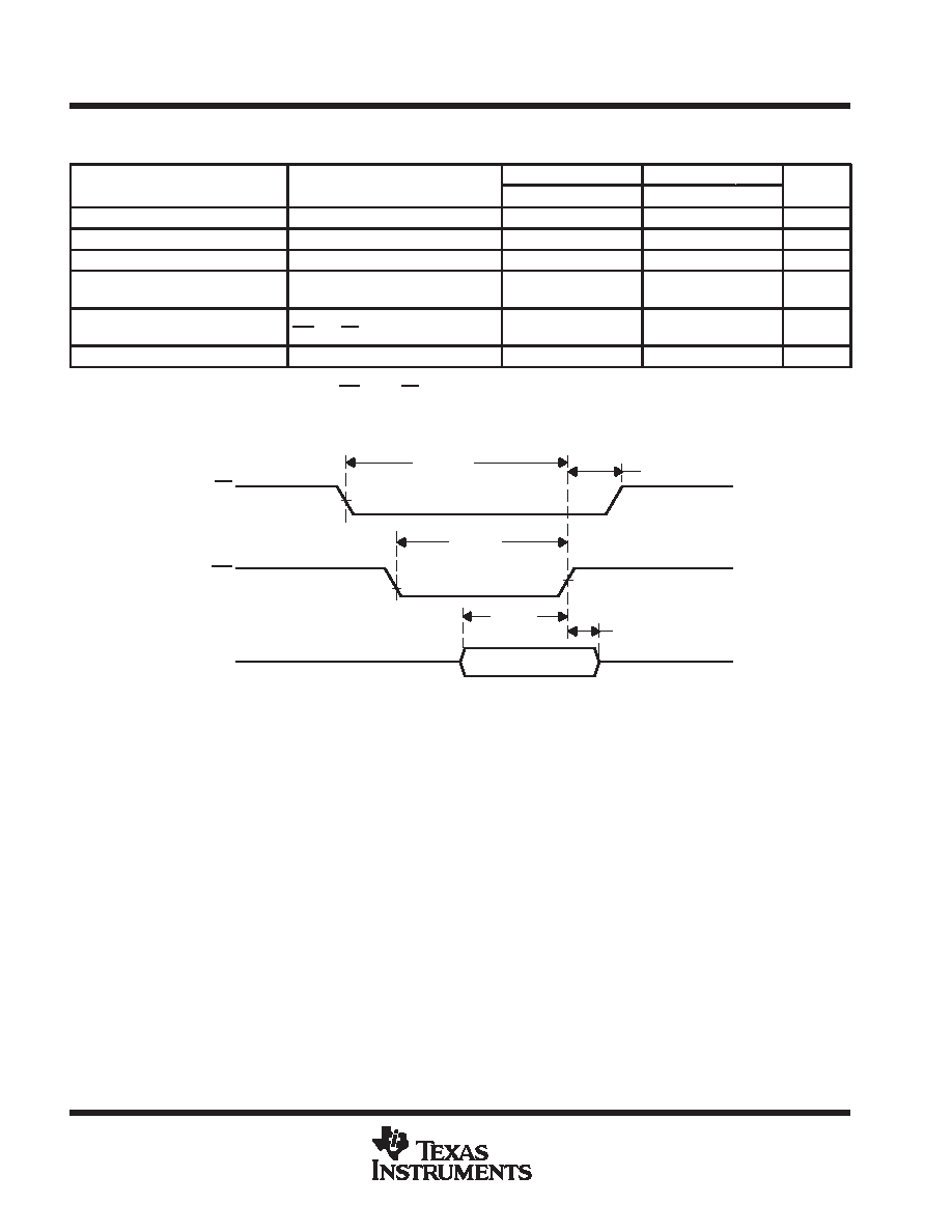
operating sequence
DB0–DB7
WR
CS
th(D)
tsu(D)
tw(WR)
th(CS)
tsu(CS)
發(fā)布緊急采購(gòu),3分鐘左右您將得到回復(fù)。