- 您現在的位置:買賣IC網 > PDF目錄373911 > AD7660AST (ANALOG DEVICES INC) 16-Bit, 100 kSPS CMOS ADC PDF資料下載
參數資料
| 型號: | AD7660AST |
| 廠商: | ANALOG DEVICES INC |
| 元件分類: | ADC |
| 英文描述: | 16-Bit, 100 kSPS CMOS ADC |
| 中文描述: | 1-CH 16-BIT SUCCESSIVE APPROXIMATION ADC, SERIAL/PARALLEL ACCESS, PQFP48 |
| 封裝: | MS-026BBC, LQFP-48 |
| 文件頁數: | 4/20頁 |
| 文件大小: | 218K |
| 代理商: | AD7660AST |
REV. 0
AD7660
–4–
ABSOLUTE MAXIMUM RATINGS
1
Analog Inputs
IN
2
, REF . . . . . . . . . . . . AVDD + 0.3 V to AGND – 0.3 V
INGND, REFGND . . . . . . . . . . . . . . . . . . AGND
±
0.3 V
Ground Voltage Differences
AGND, DGND, OGND . . . . . . . . . . . . . . . . . . . . .
±
0.3 V
Supply Voltages
AVDD, DVDD, OVDD . . . . . . . . . . . . . . . . . . . . . . . . 7 V
AVDD to DVDD,
AVDD to OVDD . . . . . . . . . . . . . .
±
7 V
DVDD to OVDD . . . . . . . . . . . . . . . . . . . . . . . . . . . .
±
7 V
Digital Inputs
Except the Data Bus D(7:4) . . . –0.3 V to DVDD + 0.3 V
Data Bus Inputs D(7:4) . . . . . . –0.3 V to OVDD + 0.3 V
Internal Power Dissipation
3
. . . . . . . . . . . . . . . . . . . 700 mW
Junction Temperature . . . . . . . . . . . . . . . . . . . . . . . . . . 150
°
C
Storage Temperature Range . . . . . . . . . . . . –65
°
C to +150
°
C
Lead Temperature Range
(Soldering 10 sec) . . . . . . . . . . . . . . . . . . . . . . . . . . . 300
°
C
NOTES
1
Stresses above those listed under Absolute Maximum Ratings may cause perma-
nent damage to the device. This is a stress rating only; functional operation of the
device at these or any other conditions above those indicated in the operational
section of this specification is not implied. Exposure to absolute maximum rating
conditions for extended periods may affect device reliability.
2
See Analog Input section.
3
Specification is for device in free air: 48-Lead LQFP:
θ
JA
= 91
°
C/W,
θ
JC
= 30
°
C/W.
I
OH
500 A
1.6mA
I
OL
TO OUTPUT
PIN
1.4V
C
L
60pF
1
NOTE:
1
IN SERIAL INTERFACE MODES, THE SYNC, SCLK, AND
SDOUT TIMINGS ARE DEFINED WITH A MAXIMUM LOAD
C
L
OF 10pF; OTHERWISE, THE LOAD IS 60pF MAXIMUM.
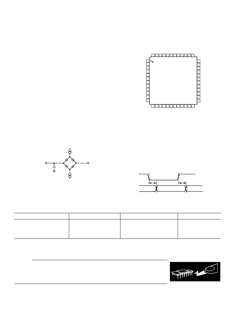
Figure 1. Load Circuit for Digital Interface Timing
CAUTION
ESD (electrostatic discharge) sensitive device. Electrostatic charges as high as 4000 V readily
accumulate on the human body and test equipment and can discharge without detection. Although
the AD7660 features proprietary ESD protection circuitry, permanent damage may occur on
devices subjected to high-energy electrostatic discharges. Therefore, proper ESD precautions are
recommended to avoid performance degradation or loss of functionality.
WARNING!
ESD SENSITIVE DEVICE
ORDERING GUIDE
Model
Temperature Range
–40
°
C to +85
°
C
–40
°
C to +85
°
C
Package Description
Package Option
AD7660AST
AD7660ASTRL
EVAL-AD7660CB
1
EVAL-CONTROL BOARD
2
Quad Flatpack (LQFP)
Quad Flatpack (LQFP)
Evaluation Board
Controller Board
ST-48
ST-48
NOTES
1
This board can be used as a stand-alone evaluation board or in conjunction with the EVAL-CONTROL BOARD for evaluation/demonstration purposes.
2
This board allows a PC to control and communicate with all Analog Devices evaluation boards ending in the CB designators.
36
35
34
33
32
31
30
29
28
27
26
25
13 14 15 16 17 18 19 20 21 22 23 24
D
I
1
2
3
4
5
6
7
8
9
10
11
12
48 47 46 45 44
39 38 37
43 42 41 40
PIN 1
TOP VIEW
(Not to Scale)
AGND
CNVST
PD
RESET
CS
RD
DGND
BUSY
D15
D14
D13
D12
AGND
AVDD
NC
DGND
OB/
2C
NC
NC
NC = NO CONNECT
SER/
PAR
D0
D1
D2
D3
AD7660
D
D
D
O
O
D
D
D
D
D
D
N
N
N
N
N
N
N
N
N
I
R
R
PIN CONFIGURATION
48-Lead LQFP
(ST-48)
t
DELAY
t
DELAY
2V
0.8V
0.8V
0.8V
2V
2V
Figure 2. Voltage Reference Levels for Timings
相關PDF資料 |
PDF描述 |
|---|---|
| AD7660ASTRL | 16-Bit, 100 kSPS CMOS ADC |
| AD7664 | Circular Connector; No. of Contacts:4; Series:D38999; Body Material:Metal; Connecting Termination:Crimp; Connector Shell Size:13; Circular Contact Gender:Socket; Circular Shell Style:Straight Plug; Insert Arrangement:13-4 |
| AD7664ASTRL | 16-Bit, 570 kSPS CMOS ADC |
| AD7664AST | 16-Bit, 570 kSPS CMOS ADC |
| AD7665 | TV 8C 8#20 PIN PLUG |
相關代理商/技術參數 |
參數描述 |
|---|---|
| AD7660ASTRL | 制造商:Analog Devices 功能描述:ADC Single SAR 100ksps 16-bit Parallel/Serial 48-Pin LQFP T/R |
| AD7660ASTRLZ | 制造商:Analog Devices 功能描述:ADC Single SAR 100ksps 16-bit Parallel/Serial 48-Pin LQFP T/R |
| AD7660ASTZ | 功能描述:IC ADC 16BIT UNIPOLAR 48-LQFP RoHS:是 類別:集成電路 (IC) >> 數據采集 - 模數轉換器 系列:PulSAR® 標準包裝:1 系列:microPOWER™ 位數:8 采樣率(每秒):1M 數據接口:串行,SPI? 轉換器數目:1 功率耗散(最大):- 電壓電源:模擬和數字 工作溫度:-40°C ~ 125°C 安裝類型:表面貼裝 封裝/外殼:24-VFQFN 裸露焊盤 供應商設備封裝:24-VQFN 裸露焊盤(4x4) 包裝:Digi-Reel® 輸入數目和類型:8 個單端,單極 產品目錄頁面:892 (CN2011-ZH PDF) 其它名稱:296-25851-6 |
| AD7660ASTZ | 制造商:Analog Devices 功能描述:IC 16-BIT ADC |
| AD7660ASTZRL | 功能描述:IC ADC 16BIT UNIPOLAR 48LQFP RoHS:是 類別:集成電路 (IC) >> 數據采集 - 模數轉換器 系列:PulSAR® 標準包裝:1,000 系列:- 位數:12 采樣率(每秒):300k 數據接口:并聯 轉換器數目:1 功率耗散(最大):75mW 電壓電源:單電源 工作溫度:0°C ~ 70°C 安裝類型:表面貼裝 封裝/外殼:24-SOIC(0.295",7.50mm 寬) 供應商設備封裝:24-SOIC 包裝:帶卷 (TR) 輸入數目和類型:1 個單端,單極;1 個單端,雙極 |
發布緊急采購,3分鐘左右您將得到回復。