- 您現在的位置:買賣IC網 > PDF目錄373927 > AD7923BRU (ANALOG DEVICES INC) Four Wall Header; No. of Contacts:60; Pitch Spacing:0.1"; No. of Rows:2; Gender:Header; Body Material:Glass-filled Polyester; Contact Plating:Nickel; Leaded Process Compatible:No; Mounting Type:Through Hole RoHS Compliant: No PDF資料下載
參數資料
| 型號: | AD7923BRU |
| 廠商: | ANALOG DEVICES INC |
| 元件分類: | ADC |
| 英文描述: | Four Wall Header; No. of Contacts:60; Pitch Spacing:0.1"; No. of Rows:2; Gender:Header; Body Material:Glass-filled Polyester; Contact Plating:Nickel; Leaded Process Compatible:No; Mounting Type:Through Hole RoHS Compliant: No |
| 中文描述: | 4-CH 12-BIT SUCCESSIVE APPROXIMATION ADC, SERIAL ACCESS, PDSO16 |
| 封裝: | MO-153AB, TSSOP-16 |
| 文件頁數: | 18/20頁 |
| 文件大小: | 430K |
| 代理商: | AD7923BRU |
–18–
AD7923
REV. 0
Writing information to the Control Register takes place on the
first 12 falling edges of SCLK in a data transfer, assuming the
MSB, i.e., the WRITE bit, has been set to 1.
The 16-bit word read from the AD7923 will always contain two
leading zeros, two channel address bits that the conversion
result corresponds to, followed by the 12-bit conversion result.
Writing Between Conversions
As outlined in the Operating Modes section, not less than 5
m
s
should be left between consecutive valid conversions; however
there is one case where this does not necessarily mean that at
least 5
m
s should always be left between
CS
falling edges.
Con-
sider the case when writing to the AD7923 to power it up from
shutdown prior to a valid conversion. The user must write to the
part to tell it to power up before it can convert successfully.
Once the serial write to power up has finished, one may want to
perform the conversion as soon as possible and not have to wait
an additional 5
m
s before bringing
CS
low for the conversion. In
this case, as long as there is a minimum of 5
m
s between each
valid
conversion, only the quiet time between the
CS
rising edge at
the end of the write to power up and the next
CS
falling edge
for a valid conversion needs to be met. Figure 17 illustrates
this point. Note that when writing to the AD7923 between these
valid conversions, the DOUT line will not be driven during the
extra write operation.
It is critical that an extra write operation as outlined above is never
issued between valid conversions when the AD7923 is executing
through a sequence function, because the falling edge of
CS
in
the extra write would move the mux onto the next channel in
the sequence. This means when the next valid conversion takes
place a channel result would have been missed.
MICROPROCESSOR INTERFACING
The serial interface on the AD7923 allows the part to be directly
connected to a range of many different microprocessors. This
section explains how to interface the AD7923 with some of
the more common microcontroller and DSP serial interface
protocols.
AD7923 to TMS320C541
The serial interface on the TMS320C541 uses a continuous
serial clock and frame synchronization signals to synchronize
the data transfer operations with peripheral devices like the
AD7923. The
CS
input allows easy interfacing between the
TMS320C541 and the AD7923 without any glue logic required.
The serial port of the TMS320C541 is set up to operate in burst
mode with internal CLKX0 (Tx serial clock on serial port 0) and
FSX0 (Tx frame sync from serial port 0). The serial port control
register (SPC) must have the following setup: FO = 0, FSM = 1,
MCM = 1, and TXM = 1. The connection diagram is shown in
Figure 18. It should be noted that for signal processing applica-
tions, it is imperative that the frame synchronization signal from
the TMS320C541 provides equidistant sampling. The V
DRIVE
pin of the AD7923 takes the same supply voltage as that of the
TMS320C541. This allows the ADC to operate at a higher
voltage than the serial interface, i.e., TMS320C541, if necessary.
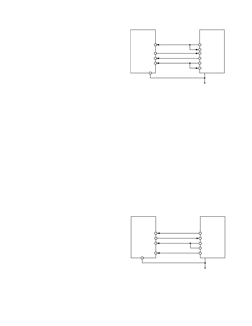
TMS320C541
*
AD7923
*
CLKX
CLKR
DR
DT
FSX
FSR
V
DD
SCLK
DOUT
DIN
CS
V
DRIVE
*
ADDITIONAL PINS REMOVED FOR CLARITY
Figure 18. Interfacing to the TMS320C541
AD7923 to ADSP-21xx
The ADSP-21xx family of DSPs is interfaced directly to the
AD7923 without any glue logic required. The V
DRIVE
pin of the
AD7923 takes the same supply voltage as that of the ADSP-218x.
This allows the ADC to operate at a higher voltage than the
serial interface, i.e., ADSP-218x, if necessary.
The SPORT0 Control Register should be set up as follows:
TFSW = RFSW = 1, Alternate Framing
INVRFS = INVTFS = 1, Active Low Frame Signal
DTYPE = 00, Right Justify Data
SLEN = 1111, 16-Bit Data-Words
ISCLK = 1, Internal Serial Clock
TFSR = RFSR = 1, Frame Every Word
IRFS = 0
ITFS = 1
The connection diagram is shown in Figure 19. The ADSP-218x
has the TFS and RFS of the SPORT tied together, with TFS set
as an output and RFS set as an input. The DSP operates in
Alternate Framing Mode and the SPORT Control Register is
set up as described. The frame synchronization signal generated
on the TFS is tied to
CS
and, as with all signal processing appli-
cations, equidistant sampling is necessary. However, in this
example, the timer interrupt is used to control the sampling rate
of the ADC, and under certain conditions equidistant sampling
may not be achieved.
AD7923
*
ADSP-218x
*
SCLK
DR
RFS
TFS
DT
V
DD
SCLK
DOUT
CS
DIN
V
DRIVE
*
ADDITIONAL PINS REMOVED FOR CLARITY
Figure 19. Interfacing to the ADSP-218x
相關PDF資料 |
PDF描述 |
|---|---|
| AD7940BRJ-R2 | 3mW, 100kSPS, 14-Bit ADC in 6-Lead SOT-23 |
| AD7947 | 3mW, 100kSPS, 14-Bit ADC in 6-Lead SOT-23 |
| AD7940BRJ-REEL7 | 3mW, 100kSPS, 14-Bit ADC in 6-Lead SOT-23 |
| AD7680 | 3mW, 100kSPS, 14-Bit ADC in 6-Lead SOT-23 |
| AD7683 | 3mW, 100kSPS, 14-Bit ADC in 6-Lead SOT-23 |
相關代理商/技術參數 |
參數描述 |
|---|---|
| AD7923BRU-REEL | 制造商:Analog Devices 功能描述:ADC Single SAR 200ksps 12-bit Serial 16-Pin TSSOP T/R 制造商:Analog Devices 功能描述:ADC SGL SAR 200KSPS 12-BIT SERL 16TSSOP - Tape and Reel |
| AD7923BRU-REEL7 | 制造商:Analog Devices 功能描述:ADC Single SAR 200ksps 12-bit Serial 16-Pin TSSOP T/R |
| AD7923BRUZ | 功能描述:IC ADC 12BIT 4CH W/SEQ 16TSSOP RoHS:是 類別:集成電路 (IC) >> 數據采集 - 模數轉換器 系列:- 標準包裝:1 系列:microPOWER™ 位數:8 采樣率(每秒):1M 數據接口:串行,SPI? 轉換器數目:1 功率耗散(最大):- 電壓電源:模擬和數字 工作溫度:-40°C ~ 125°C 安裝類型:表面貼裝 封裝/外殼:24-VFQFN 裸露焊盤 供應商設備封裝:24-VQFN 裸露焊盤(4x4) 包裝:Digi-Reel® 輸入數目和類型:8 個單端,單極 產品目錄頁面:892 (CN2011-ZH PDF) 其它名稱:296-25851-6 |
| AD7923BRUZ-REEL | 功能描述:IC ADC 12BIT 4CH W/SEQ 16TSSOP RoHS:是 類別:集成電路 (IC) >> 數據采集 - 模數轉換器 系列:- 標準包裝:2,500 系列:- 位數:16 采樣率(每秒):15 數據接口:MICROWIRE?,串行,SPI? 轉換器數目:1 功率耗散(最大):480µW 電壓電源:單電源 工作溫度:-40°C ~ 85°C 安裝類型:表面貼裝 封裝/外殼:38-WFQFN 裸露焊盤 供應商設備封裝:38-QFN(5x7) 包裝:帶卷 (TR) 輸入數目和類型:16 個單端,雙極;8 個差分,雙極 配用:DC1011A-C-ND - BOARD DELTA SIGMA ADC LTC2494 |
| AD7923BRUZ-REEL7 | 功能描述:IC ADC 12BIT 4CH W/SEQ 16TSSOP RoHS:是 類別:集成電路 (IC) >> 數據采集 - 模數轉換器 系列:- 標準包裝:1 系列:microPOWER™ 位數:8 采樣率(每秒):1M 數據接口:串行,SPI? 轉換器數目:1 功率耗散(最大):- 電壓電源:模擬和數字 工作溫度:-40°C ~ 125°C 安裝類型:表面貼裝 封裝/外殼:24-VFQFN 裸露焊盤 供應商設備封裝:24-VQFN 裸露焊盤(4x4) 包裝:Digi-Reel® 輸入數目和類型:8 個單端,單極 產品目錄頁面:892 (CN2011-ZH PDF) 其它名稱:296-25851-6 |
發布緊急采購,3分鐘左右您將得到回復。