- 您現在的位置:買賣IC網 > PDF目錄375885 > FQI65N06 (FAIRCHILD SEMICONDUCTOR CORP) 60V N-Channel MOSFET PDF資料下載
參數資料
| 型號: | FQI65N06 |
| 廠商: | FAIRCHILD SEMICONDUCTOR CORP |
| 元件分類: | JFETs |
| 英文描述: | 60V N-Channel MOSFET |
| 中文描述: | 65 A, 60 V, 0.016 ohm, N-CHANNEL, Si, POWER, MOSFET, TO-262 |
| 封裝: | I2PAK-3 |
| 文件頁數: | 1/9頁 |
| 文件大小: | 668K |
| 代理商: | FQI65N06 |
May 2001
QF E T
TM
F
2001 Fairchild Semiconductor Corporation
Rev. A1. May 2001
FQB65N06 / FQI65N06
60V N-Channel MOSFET
General Description
These N-Channel enhancement mode power field effect
transistors are produced using Fairchild’s proprietary,
planar stripe, DMOS technology.
This advanced technology has been especially tailored to
minimize on-state resistance, provide superior switching
performance, and withstand high energy pulse in the
avalanche and commutation mode. These devices are well
suited for low voltage applications such as automotive, DC/
DC converters, and high efficiency switching for power
management in portable and battery operated products.
Features
65A, 60V, R
DS(on)
= 0.016
@V
GS
= 10 V
Low gate charge ( typical 48 nC)
Low Crss ( typical 100 pF)
Fast switching
100% avalanche tested
Improved dv/dt capability
175
°
C maximum junction temperature rating
! "
!
!
S
!
"
"
Absolute Maximum Ratings
T
C
= 25°C unless otherwise noted
Thermal Characteristics
Symbol
V
DSS
I
D
Parameter
FQB65N06 / FQI65N06
60
65
46.1
260
±
25
650
65
15.0
7.0
3.75
150
1.00
-55 to +175
Units
V
A
A
A
V
mJ
A
mJ
V/ns
W
W
W/°C
°C
Drain-Source Voltage
Drain Current
- Continuous (T
C
= 25°C)
- Continuous (T
C
= 100°C)
- Pulsed
I
DM
V
GSS
E
AS
I
AR
E
AR
dv/dt
P
D
Drain Current
Gate-Source Voltage
Single Pulsed Avalanche Energy
Avalanche Current
Repetitive Avalanche Energy
Peak Diode Recovery dv/dt
Power Dissipation (T
A
= 25°C) *
Power Dissipation (T
C
= 25°C)
(Note 1)
(Note 2)
(Note 1)
(Note 1)
(Note 3)
- Derate above 25°C
T
J
, T
stg
Operating and Storage Temperature Range
Maximum lead temperature for soldering purposes,
1/8
"
from case for 5 seconds
T
L
300
°C
Symbol
R
θ
JC
R
θ
JA
R
θ
JA
* When mounted on the minimum pad size recommended (PCB Mount)
Parameter
Typ
--
--
--
Max
1.00
40
62.5
Units
°C
/
W
°C
/
W
°C
/
W
Thermal Resistance, Junction-to-Case
Thermal Resistance, Junction-to-Ambient *
Thermal Resistance, Junction-to-Ambient
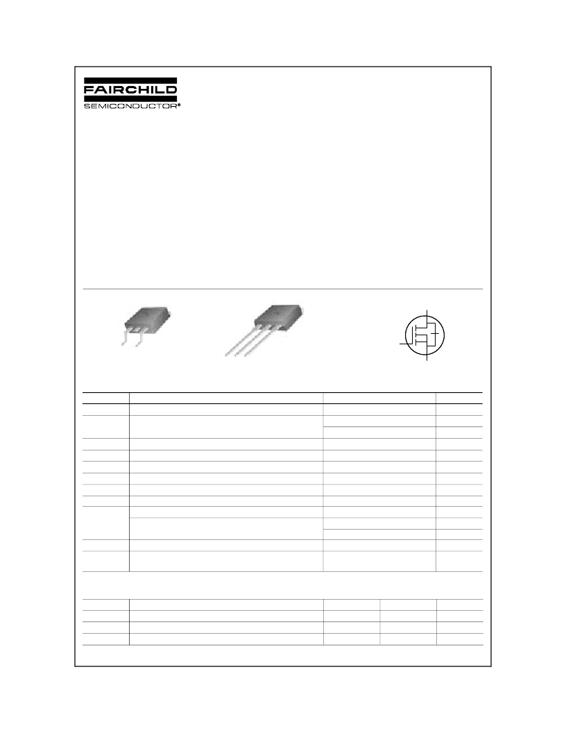
D
G
D
2
-PAK
FQB Series
I
2
-PAK
FQI Series
G
S
D
G
S
D
相關PDF資料 |
PDF描述 |
|---|---|
| FQB65N06 | 60V N-Channel MOSFET |
| FQI6N15 | 150V N-Channel MOSFET |
| FQB6N15 | 150V N-Channel MOSFET |
| FQI6N25 | 250V N-Channel MOSFET |
| FQB6N25 | 250V N-Channel MOSFET |
相關代理商/技術參數 |
參數描述 |
|---|---|
| FQI6N15 | 制造商:FAIRCHILD 制造商全稱:Fairchild Semiconductor 功能描述:150V N-Channel MOSFET |
| FQI6N15TU | 功能描述:MOSFET N-CH/150V/6.3A/0.65OHM RoHS:否 制造商:STMicroelectronics 晶體管極性:N-Channel 汲極/源極擊穿電壓:650 V 閘/源擊穿電壓:25 V 漏極連續電流:130 A 電阻汲極/源極 RDS(導通):0.014 Ohms 配置:Single 最大工作溫度: 安裝風格:Through Hole 封裝 / 箱體:Max247 封裝:Tube |
| FQI6N25 | 制造商:FAIRCHILD 制造商全稱:Fairchild Semiconductor 功能描述:250V N-Channel MOSFET |
| FQI6N40 | 制造商:FAIRCHILD 制造商全稱:Fairchild Semiconductor 功能描述:400V N-Channel MOSFET |
| FQI6N40C | 制造商:FAIRCHILD 制造商全稱:Fairchild Semiconductor 功能描述:400V N-Channel MOSFET |
發布緊急采購,3分鐘左右您將得到回復。