- 您現在的位置:買賣IC網 > PDF目錄373917 > AD7810 (Analog Devices, Inc.) 2.7 V to 5.5 V, 2 us, 10-Bit ADC in 8-Lead microSOIC/DIP PDF資料下載
參數資料
| 型號: | AD7810 |
| 廠商: | Analog Devices, Inc. |
| 英文描述: | 2.7 V to 5.5 V, 2 us, 10-Bit ADC in 8-Lead microSOIC/DIP |
| 中文描述: | 2.7 V至5.5 V,2我們,10位ADC的8引腳microSOIC /文憑 |
| 文件頁數: | 8/11頁 |
| 文件大小: | 142K |
| 代理商: | AD7810 |
AD7810
–8–
REV. A
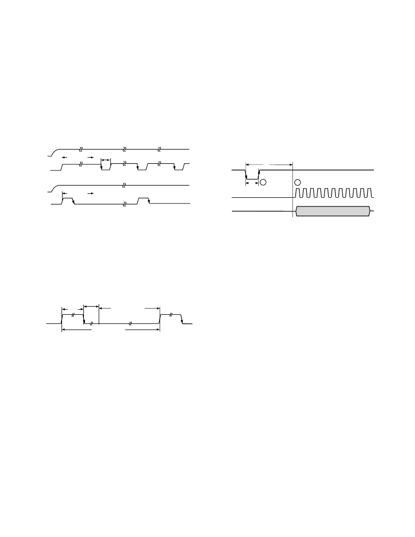
POWER-UP TIMES
The AD7810 has a 1
μ
s power-up time. When V
DD
is first con-
nected, the AD7810 is in a low current mode of operation. In
order to carry out a conversion, the AD7810 must first be pow-
ered up. The ADC is powered up by a rising edge on the
CONVST
pin. A conversion is initiated on the falling edge of
CONVST
. Figure 12 shows how to power up the AD7810 when
V
DD
is first connected or after the AD7810 is powered down
using the
CONVST
pin.
Care must be taken to ensure that the
CONVST
pin of the
AD7810 is logic low when V
DD
is first applied.
MODE 1 (
CONVST
IDLES HIGH)
V
DD
MODE 2 (
CONVST
IDLES LOW)
V
DD
< 1
m
s
t
POWER-UP
m
t
POWER-UP
m
CONVST
CONVST
Figure 12. Power-Up Times
POWER VS. THROUGHPUT RATE
By operating the AD7810 in Mode 2, the average power con-
sumption of the AD7810 decreases at lower throughput rates.
Figure 13 shows how the automatic power-down is implemented
using the
CONVST
signal to achieve the optimum power per-
formance for the AD7810. As the throughput rate is reduced, the
device remains in its power-down state longer and the average
power consumption over time drops accordingly.
t
100
m
s @ 10kSPS
CONVST
t
CONVERT
2
m
s
POWER-DOWN
t
POWER-UP
1
m
s
Figure 13. Automatic Power-Down
For example, if the AD7810 is operated in a continuous sam-
pling mode with a throughput rate of 10 kSPS, the power con-
sumption is calculated as follows. The power dissipation during
normal operation is 9 mW, V
DD
= 3 V. If the power-up time is
1
μ
s and the conversion time is 2
μ
s, the AD7810 can be said to
dissipate 9 mW for 3
μ
s (worst case) during each conversion
cycle. If the throughput rate is 10 kSPS, the cycle time is
100
μ
s and the average power dissipated during each cycle is
(3/100)
×
(9 mW) = 270
μ
W. Figure 2 shows a graph of Power
vs. Throughput.
OPERATING MODES
Mode 1 Operation (High Speed Sampling)
When the AD7810 is used in this mode of operation, the part is
not powered down between conversions. This mode of opera-
tion allows high throughput rates to be achieved. The timing
diagram in Figure 14 shows how this optimum throughput rate
is achieved by bringing the
CONVST
signal high before the end
of the conversion. The AD7810 leaves its tracking mode and
goes into hold on the falling edge of
CONVST
. A conversion is
also initiated at this time. The conversion takes 2
μ
s to complete.
At this point, the result of the current conversion is latched into the
serial shift register, and the state of the
CONVST
signal checked.
The
CONVST
signal should be high at the end of the conversion
to prevent the part from powering down.
A
B
t
2
D
OUT
CURRENT CONVERSION RESULT
t
1
SCLK
CONVST
Figure 14. Mode 1 Operation Timing
The serial port on the AD7810 is enabled on the rising edge of
the
CONVST
signal (see Serial Interface section). As explained
earlier, this rising edge should occur before the end of the con-
version process if the part is not to be powered down. A serial
read can take place at any stage after the rising edge of
CONVST
. If a serial read is initiated before the end of the cur-
rent conversion process (i.e., at time “A”), the result of the
previous conversion is shifted out on the D
OUT
pin. It is possible
to allow the serial read to extend beyond the end of a conver-
sion. In this case the new data will not be latched into the out-
put shift register until the read has finished. The dynamic
performance of the AD7810 typically degrades by up to 3 dBs
while reading during a conversion. If the user waits until the
end of the conversion process, i.e., 2
μ
s after falling edge of
CONVST
(Point “B”), before initiating a read, the current
conversion result is shifted out.
相關PDF資料 |
PDF描述 |
|---|---|
| AD7810YN | 2.7 V to 5.5 V, 2 us, 10-Bit ADC in 8-Lead microSOIC/DIP |
| AD7810YR | ECONOLINE: REC2.2-S_DR/H1 - 2.2W DIP Package- 1kVDC Isolation- Regulated Output- UL94V-0 Package Material- Continuous Short Circiut Protection- Internal SMD design- 100% Burned In- Efficiency to 75% |
| AD7813YRU | +2.7 V to +5.5 V, 400 kSPS 8-/10-Bit Sampling ADC |
| AD7813YN | +2.7 V to +5.5 V, 400 kSPS 8-/10-Bit Sampling ADC |
| AD7813YR | +2.7 V to +5.5 V, 400 kSPS 8-/10-Bit Sampling ADC |
相關代理商/技術參數 |
參數描述 |
|---|---|
| AD7810YN | 制造商:Analog Devices 功能描述:ADC Single SAR 350ksps 10-bit Serial 8-Pin PDIP 制造商:Rochester Electronics LLC 功能描述:10-BIT SERIAL SINGLE ADC I.C. - Bulk 制造商:Analog Devices 功能描述:IC 10-BIT ADC |
| AD7810YNZ | 功能描述:IC ADC 10BIT SRL HS LP 8DIP RoHS:是 類別:集成電路 (IC) >> 數據采集 - 模數轉換器 系列:- 其它有關文件:TSA1204 View All Specifications 標準包裝:1 系列:- 位數:12 采樣率(每秒):20M 數據接口:并聯 轉換器數目:2 功率耗散(最大):155mW 電壓電源:模擬和數字 工作溫度:-40°C ~ 85°C 安裝類型:表面貼裝 封裝/外殼:48-TQFP 供應商設備封裝:48-TQFP(7x7) 包裝:Digi-Reel® 輸入數目和類型:4 個單端,單極;2 個差分,單極 產品目錄頁面:1156 (CN2011-ZH PDF) 其它名稱:497-5435-6 |
| AD7810YR | 功能描述:IC ADC 10BIT 2.7V 8-SOIC RoHS:否 類別:集成電路 (IC) >> 數據采集 - 模數轉換器 系列:- 產品培訓模塊:Lead (SnPb) Finish for COTS Obsolescence Mitigation Program 標準包裝:2,500 系列:- 位數:12 采樣率(每秒):3M 數據接口:- 轉換器數目:- 功率耗散(最大):- 電壓電源:- 工作溫度:- 安裝類型:表面貼裝 封裝/外殼:SOT-23-6 供應商設備封裝:SOT-23-6 包裝:帶卷 (TR) 輸入數目和類型:- |
| AD7810YRM | 制造商:Analog Devices 功能描述:ADC Single SAR 350ksps 10-bit Serial 8-Pin MSOP 制造商:Rochester Electronics LLC 功能描述:10-BIT SERIAL SINGLE ADC I.C. - Bulk |
| AD7810YRM-REEL | 制造商:Analog Devices 功能描述:ADC Single SAR 350ksps 10-bit Serial 8-Pin MSOP T/R |
發布緊急采購,3分鐘左右您將得到回復。