- 您現在的位置:買賣IC網 > PDF目錄363900 > W79E227A (WINBOND ELECTRONICS CORP) 8-BIT MICROCONTROLLER PDF資料下載
參數資料
| 型號: | W79E227A |
| 廠商: | WINBOND ELECTRONICS CORP |
| 元件分類: | 8位微控制器 |
| 英文描述: | 8-BIT MICROCONTROLLER |
| 中文描述: | 8位微控制器 |
| 文件頁數: | 39/200頁 |
| 文件大小: | 3644K |
| 代理商: | W79E227A |
第1頁第2頁第3頁第4頁第5頁第6頁第7頁第8頁第9頁第10頁第11頁第12頁第13頁第14頁第15頁第16頁第17頁第18頁第19頁第20頁第21頁第22頁第23頁第24頁第25頁第26頁第27頁第28頁第29頁第30頁第31頁第32頁第33頁第34頁第35頁第36頁第37頁第38頁當前第39頁第40頁第41頁第42頁第43頁第44頁第45頁第46頁第47頁第48頁第49頁第50頁第51頁第52頁第53頁第54頁第55頁第56頁第57頁第58頁第59頁第60頁第61頁第62頁第63頁第64頁第65頁第66頁第67頁第68頁第69頁第70頁第71頁第72頁第73頁第74頁第75頁第76頁第77頁第78頁第79頁第80頁第81頁第82頁第83頁第84頁第85頁第86頁第87頁第88頁第89頁第90頁第91頁第92頁第93頁第94頁第95頁第96頁第97頁第98頁第99頁第100頁第101頁第102頁第103頁第104頁第105頁第106頁第107頁第108頁第109頁第110頁第111頁第112頁第113頁第114頁第115頁第116頁第117頁第118頁第119頁第120頁第121頁第122頁第123頁第124頁第125頁第126頁第127頁第128頁第129頁第130頁第131頁第132頁第133頁第134頁第135頁第136頁第137頁第138頁第139頁第140頁第141頁第142頁第143頁第144頁第145頁第146頁第147頁第148頁第149頁第150頁第151頁第152頁第153頁第154頁第155頁第156頁第157頁第158頁第159頁第160頁第161頁第162頁第163頁第164頁第165頁第166頁第167頁第168頁第169頁第170頁第171頁第172頁第173頁第174頁第175頁第176頁第177頁第178頁第179頁第180頁第181頁第182頁第183頁第184頁第185頁第186頁第187頁第188頁第189頁第190頁第191頁第192頁第193頁第194頁第195頁第196頁第197頁第198頁第199頁第200頁
Preliminary W79E225A/227A Data Sheet
Publication Release Date: December 14, 2007
- 39 -
Revision A2.0
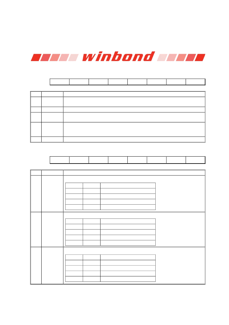
PORT 4 CHIP-SELECT POLARITY
Bit:
7
6
5
4
3
2
1
0
P43INV
P42INV
P41INV
P40INV
-
PWDNH
RMWFP
PUP0
Mnemonic: P4CSIN
Address: A2h
BIT
NAME
FUNCTION
7-4
P4xINV
The Active Polarity of P4.x when it is set as a chip-select strobe output. High =
Active High. Low = Active Low. Note: x = 3,2,1,0.
Reserved.
Set PWDNH to logic 1 then ALE and PSEN will keep high state, clear this bit to
logic 0 then ALE and PSEN will output low during power down mode.
Control Read Path of Instruction “Read-Modify-Write”. When this bit is set, the
read path of executing “read-modify-write” instruction is from port pin otherwise
from SFR.
Enable Port 0 weak pull up.
3
-
2
PWDNH
1
RMWFP
0
PUP0
CAPTURE CONTROL 0 REGISTER
Bit:
7
6
5
4
3
2
1
0
CCT2.1
CCT2.0
CCT1.1
CCT1.0
CCT0.1
CCT0.0
CCLD1
CCLD0
Mnemonic: CAPCON0
Address: A3h
BIT
NAME
FUNCTION
7-6
CCT2.1-0
Capture 2 edge select.
CCT2.1 CCT2.0
0
0
1
1
Description
0
1
0
1
Rising edge trigger
Falling edge trigger
Rising and falling edge trigger
Reserved.
5-4
CCT1.1-0
Capture 1 edge select.
CCT1.1 CCT1.0
0
0
1
1
Description
0
1
0
1
Rising edge trigger
Falling edge trigger
Rising and falling edge trigger
Reserved.
3-2
CCT0.1-0
Capture 0 edge select.
CCT0.1 CCT0.0
0
0
1
1
Description
0
1
0
1
Rising edge trigger
Falling edge trigger
Rising and falling edge trigger
Reserved.
相關PDF資料 |
PDF描述 |
|---|---|
| W79E227AFG | 8-BIT MICROCONTROLLER |
| W79E227APG | 8-BIT MICROCONTROLLER |
| W79E532 | 8-BIT MICROCONTROLLER |
| W79E532A40DL | 8-BIT MICROCONTROLLER |
| W79E532A40DN | 8-BIT MICROCONTROLLER |
相關代理商/技術參數 |
參數描述 |
|---|---|
| W79E227AFG | 制造商:WINBOND 制造商全稱:Winbond 功能描述:8-bit Microcontroller |
| W79E227ALG | 制造商:Nuvoton Technology Corp 功能描述:IC MCU 64K EPROM FLASH 48LQFP |
| W79E227APG | 制造商:Nuvoton Technology Corp 功能描述:IC MCU 64K EPROM FLASH 44PLCC |
| W79E342 | 制造商:WINBOND 制造商全稱:Winbond 功能描述:W79E342 datasheet |
| W79E4051_2051 | 制造商:WINBOND 制造商全稱:Winbond 功能描述:W79E4051_2051_SC7(中文) |
發布緊急采購,3分鐘左右您將得到回復。