- 您現(xiàn)在的位置:買賣IC網(wǎng) > PDF目錄293778 > 28229-14 (MINDSPEED TECHNOLOGIES INC) ATM/SONET/SDH SUPPORT CIRCUIT, PBGA256 PDF資料下載
參數(shù)資料
| 型號: | 28229-14 |
| 廠商: | MINDSPEED TECHNOLOGIES INC |
| 元件分類: | 數(shù)字傳輸電路 |
| 英文描述: | ATM/SONET/SDH SUPPORT CIRCUIT, PBGA256 |
| 封裝: | BGA-256 |
| 文件頁數(shù): | 207/269頁 |
| 文件大小: | 3376K |
| 代理商: | 28229-14 |
第1頁第2頁第3頁第4頁第5頁第6頁第7頁第8頁第9頁第10頁第11頁第12頁第13頁第14頁第15頁第16頁第17頁第18頁第19頁第20頁第21頁第22頁第23頁第24頁第25頁第26頁第27頁第28頁第29頁第30頁第31頁第32頁第33頁第34頁第35頁第36頁第37頁第38頁第39頁第40頁第41頁第42頁第43頁第44頁第45頁第46頁第47頁第48頁第49頁第50頁第51頁第52頁第53頁第54頁第55頁第56頁第57頁第58頁第59頁第60頁第61頁第62頁第63頁第64頁第65頁第66頁第67頁第68頁第69頁第70頁第71頁第72頁第73頁第74頁第75頁第76頁第77頁第78頁第79頁第80頁第81頁第82頁第83頁第84頁第85頁第86頁第87頁第88頁第89頁第90頁第91頁第92頁第93頁第94頁第95頁第96頁第97頁第98頁第99頁第100頁第101頁第102頁第103頁第104頁第105頁第106頁第107頁第108頁第109頁第110頁第111頁第112頁第113頁第114頁第115頁第116頁第117頁第118頁第119頁第120頁第121頁第122頁第123頁第124頁第125頁第126頁第127頁第128頁第129頁第130頁第131頁第132頁第133頁第134頁第135頁第136頁第137頁第138頁第139頁第140頁第141頁第142頁第143頁第144頁第145頁第146頁第147頁第148頁第149頁第150頁第151頁第152頁第153頁第154頁第155頁第156頁第157頁第158頁第159頁第160頁第161頁第162頁第163頁第164頁第165頁第166頁第167頁第168頁第169頁第170頁第171頁第172頁第173頁第174頁第175頁第176頁第177頁第178頁第179頁第180頁第181頁第182頁第183頁第184頁第185頁第186頁第187頁第188頁第189頁第190頁第191頁第192頁第193頁第194頁第195頁第196頁第197頁第198頁第199頁第200頁第201頁第202頁第203頁第204頁第205頁第206頁當(dāng)前第207頁第208頁第209頁第210頁第211頁第212頁第213頁第214頁第215頁第216頁第217頁第218頁第219頁第220頁第221頁第222頁第223頁第224頁第225頁第226頁第227頁第228頁第229頁第230頁第231頁第232頁第233頁第234頁第235頁第236頁第237頁第238頁第239頁第240頁第241頁第242頁第243頁第244頁第245頁第246頁第247頁第248頁第249頁第250頁第251頁第252頁第253頁第254頁第255頁第256頁第257頁第258頁第259頁第260頁第261頁第262頁第263頁第264頁第265頁第266頁第267頁第268頁第269頁
2-14
Mindspeed Technologies
28229-DSH-001-B
CX2822x Hardware Description
CX28224/5/9 Data Sheet
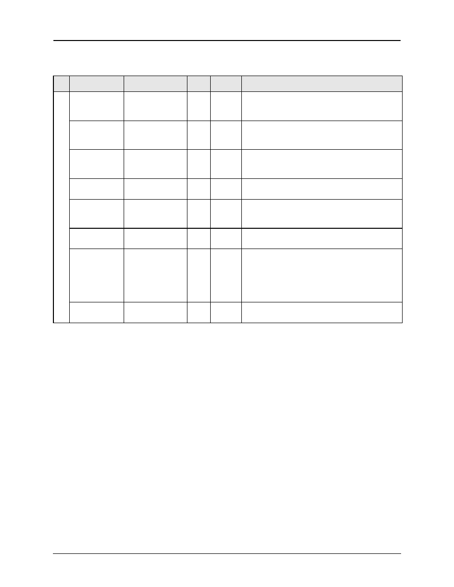
A
T
M
La
ye
r
U
T
OP
IA
Inte
rfa
ce
atmUTxClAv
ATM UTOPIA
Transmit Cell
Available
C12
O
Cell Available signal for transmit ATM cells (active high).
atmUTxSOC
ATM UTOPIA
Transmit Start of Cell
D11
I
Start of Cell synchronization signal for transmit ATM cells
(active high). Indicates that the first byte/word of the 53
byte cell is being placed on the atmUTxData bus.
atmUTxEnb*
ATM UTOPIA
Transmit Enable
B12
I
Data transfer enable for transmit ATM cells (active low).
Indicates that the first byte/word of the 53 byte cell is being
placed on the atmUTxData bus.
atmUTxClk
ATM UTOPIA
Transmit Clock
A12
I
Clock signal used for transfer of transmit ATM cells from
the ATM Layer. The maximum clock rate is 33 MHz.
atmURxSOC
ATM UTOPIA Receive
Start of Cell
C9
O
Start of Cell synchronization signal for receive ATM cells
(active high). Indicates that the first byte/word of the 53
byte cell is being placed on the atmURxData bus.
atmURxClk
ATM UTOPIA Receive
Clock
A9
I
Clock signal used for transfer of receive ATM cells from the
ATM Layer. The maximum clock rate 33 MHz.
atmURxClAv
ATM UTOPIA Receive
Cell Available
B9
O
Cell Available signal for receive ATM cells (active high). As
a software option in the IMA16 application, the pin
atmURxAdr[4] will function as a cell available status signal
(atmURxClAv[1]) for ATM Utopia addresses 8–15 only. In
this mode, atmURxClAv[1] will threestate for addresses 0–
7.
atmURxEnb*
ATM UTOPIA Receive
Enable
D8
I
Data transfer and output enable for receive ATM cells
(active low).
Table 2-3. CX2822x Pin Descriptions (9 of 12)
Pin Label
Signal Name
No.
I/O
Description
相關(guān)PDF資料 |
PDF描述 |
|---|---|
| 28230-13 | ATM SEGMENTATION AND REASSEMBLY DEVICE, PQFP208 |
| 28L0138-40R | 1 FUNCTIONS, FERRITE BEAD |
| 28L0138-70R | 1 FUNCTIONS, FERRITE BEAD |
| 28Z551 | TELECOM FILTER |
| 28Z550 | TELECOM FILTER |
相關(guān)代理商/技術(shù)參數(shù) |
參數(shù)描述 |
|---|---|
| 28-22916 | 制造商:CEBEK 功能描述:PRE ASSEMBLED MODULE BOARD PRECISION TIMER 15S-60MIN |
| 28-22918 | 制造商:CEBEK 功能描述:PRE ASSEMBLED MODULE BOARD PRECISION TIMER 0.1-10 SEC |
| 28-22920 | 制造商:CEBEK 功能描述:PRE ASSEMBLED MODULE BOARD PRECISION TIMER 1-99 SEC |
| 28-22922 | 制造商:CEBEK 功能描述:PRE ASSEMBLED MODULE BOARD SEQUENTIAL TIMER 1SEC-3MIN |
| 28-22926 | 制造商:CEBEK 功能描述:PRE ASSEMBLED MODULE BOARD ON DELAY TIMER 1-60 SECOND |
發(fā)布緊急采購,3分鐘左右您將得到回復(fù)。