- 您現在的位置:買賣IC網 > PDF目錄293778 > 28229-14 (MINDSPEED TECHNOLOGIES INC) ATM/SONET/SDH SUPPORT CIRCUIT, PBGA256 PDF資料下載
參數資料
| 型號: | 28229-14 |
| 廠商: | MINDSPEED TECHNOLOGIES INC |
| 元件分類: | 數字傳輸電路 |
| 英文描述: | ATM/SONET/SDH SUPPORT CIRCUIT, PBGA256 |
| 封裝: | BGA-256 |
| 文件頁數: | 7/269頁 |
| 文件大小: | 3376K |
| 代理商: | 28229-14 |
第1頁第2頁第3頁第4頁第5頁第6頁當前第7頁第8頁第9頁第10頁第11頁第12頁第13頁第14頁第15頁第16頁第17頁第18頁第19頁第20頁第21頁第22頁第23頁第24頁第25頁第26頁第27頁第28頁第29頁第30頁第31頁第32頁第33頁第34頁第35頁第36頁第37頁第38頁第39頁第40頁第41頁第42頁第43頁第44頁第45頁第46頁第47頁第48頁第49頁第50頁第51頁第52頁第53頁第54頁第55頁第56頁第57頁第58頁第59頁第60頁第61頁第62頁第63頁第64頁第65頁第66頁第67頁第68頁第69頁第70頁第71頁第72頁第73頁第74頁第75頁第76頁第77頁第78頁第79頁第80頁第81頁第82頁第83頁第84頁第85頁第86頁第87頁第88頁第89頁第90頁第91頁第92頁第93頁第94頁第95頁第96頁第97頁第98頁第99頁第100頁第101頁第102頁第103頁第104頁第105頁第106頁第107頁第108頁第109頁第110頁第111頁第112頁第113頁第114頁第115頁第116頁第117頁第118頁第119頁第120頁第121頁第122頁第123頁第124頁第125頁第126頁第127頁第128頁第129頁第130頁第131頁第132頁第133頁第134頁第135頁第136頁第137頁第138頁第139頁第140頁第141頁第142頁第143頁第144頁第145頁第146頁第147頁第148頁第149頁第150頁第151頁第152頁第153頁第154頁第155頁第156頁第157頁第158頁第159頁第160頁第161頁第162頁第163頁第164頁第165頁第166頁第167頁第168頁第169頁第170頁第171頁第172頁第173頁第174頁第175頁第176頁第177頁第178頁第179頁第180頁第181頁第182頁第183頁第184頁第185頁第186頁第187頁第188頁第189頁第190頁第191頁第192頁第193頁第194頁第195頁第196頁第197頁第198頁第199頁第200頁第201頁第202頁第203頁第204頁第205頁第206頁第207頁第208頁第209頁第210頁第211頁第212頁第213頁第214頁第215頁第216頁第217頁第218頁第219頁第220頁第221頁第222頁第223頁第224頁第225頁第226頁第227頁第228頁第229頁第230頁第231頁第232頁第233頁第234頁第235頁第236頁第237頁第238頁第239頁第240頁第241頁第242頁第243頁第244頁第245頁第246頁第247頁第248頁第249頁第250頁第251頁第252頁第253頁第254頁第255頁第256頁第257頁第258頁第259頁第260頁第261頁第262頁第263頁第264頁第265頁第266頁第267頁第268頁第269頁
7-4
Mindspeed Technologies
28229-DSH-001-B
Registers
CX28224/5/9 Data Sheet
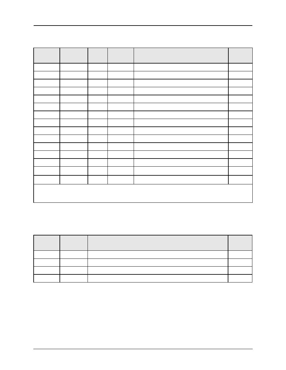
Table 7-4 lists several registers used for CX2822x’s basic functions, including device-
and port-level operating modes.
Table 7-5 lists the control registers used for transmission of traffic.
0x31
IDLCNTM
R
(2)
Idle Cell Receive Counter (middle byte)
0x32
IDLCNTH
R
(2)
Idle Cell Receive Counter (high byte)
0x33
LOCDCNT
R
(2)
LOCD Event Counter
0x34
TXCNTL
R
(2)
Transmitted Cell Counter (low byte)
0x35
TXCNTM
R
(2)
Transmitted Cell Counter (mid byte)
0x36
TXCNTH
R
(2)
Transmitted Cell Counter (high byte)
0x37
CORRCNT
R
(2)
Corrected HEC Error Counter
0x38
RXCNTL
R
(2)
Received Cell Counter (low byte)
0x39
RXCNTM
R
(2)
Received Cell Counter (mid byte)
0x3A
RXCNTH
R
(2)
Received Cell Counter (high byte)
0x3B
UNCCNT
R
(2)
Uncorrected HEC Error Counter
0x3C
NONCNTL
R
(2)
Non-Matching Cell Counter (low byte)
0x3D
NONCNTH
R
(2)
Non-Matching Cell Counter (high byte)
0x3E
—
——
Reserved, set to a logical 0
—
0x3F
—
——
Reserved, set to a logical 0
—
FOOTNOTE:
(1) One-second latching is enabled by setting EnStatLat (bit 5) in the MODE register (0x0202) to a logical 1.
(2) One-second latching is enabled by setting EnCntrLat (bit 4) in the MODE register (0x0202) to a logical 1.
Table 7-4. General Use Registers
Port Offset
Address
Name
Description
Page
Number
0x200
MODE
Device Mode Control Register
0x04
PMODE
Port Mode Control Register
0x05
IOMODE
Input/Output Mode Control Register
0x203
OUTSTAT
Output Pin Control Register
Table 7-3. Port Control and Status Registers (3 of 3)
Port Offset
Address
Name
Type
One-second
Latching
Description (Continued)
Page
Number
相關PDF資料 |
PDF描述 |
|---|---|
| 28230-13 | ATM SEGMENTATION AND REASSEMBLY DEVICE, PQFP208 |
| 28L0138-40R | 1 FUNCTIONS, FERRITE BEAD |
| 28L0138-70R | 1 FUNCTIONS, FERRITE BEAD |
| 28Z551 | TELECOM FILTER |
| 28Z550 | TELECOM FILTER |
相關代理商/技術參數 |
參數描述 |
|---|---|
| 28-22916 | 制造商:CEBEK 功能描述:PRE ASSEMBLED MODULE BOARD PRECISION TIMER 15S-60MIN |
| 28-22918 | 制造商:CEBEK 功能描述:PRE ASSEMBLED MODULE BOARD PRECISION TIMER 0.1-10 SEC |
| 28-22920 | 制造商:CEBEK 功能描述:PRE ASSEMBLED MODULE BOARD PRECISION TIMER 1-99 SEC |
| 28-22922 | 制造商:CEBEK 功能描述:PRE ASSEMBLED MODULE BOARD SEQUENTIAL TIMER 1SEC-3MIN |
| 28-22926 | 制造商:CEBEK 功能描述:PRE ASSEMBLED MODULE BOARD ON DELAY TIMER 1-60 SECOND |
發布緊急采購,3分鐘左右您將得到回復。