- 您現在的位置:買賣IC網 > PDF目錄293778 > 28229-14 (MINDSPEED TECHNOLOGIES INC) ATM/SONET/SDH SUPPORT CIRCUIT, PBGA256 PDF資料下載
參數資料
| 型號: | 28229-14 |
| 廠商: | MINDSPEED TECHNOLOGIES INC |
| 元件分類: | 數字傳輸電路 |
| 英文描述: | ATM/SONET/SDH SUPPORT CIRCUIT, PBGA256 |
| 封裝: | BGA-256 |
| 文件頁數: | 218/269頁 |
| 文件大小: | 3376K |
| 代理商: | 28229-14 |
第1頁第2頁第3頁第4頁第5頁第6頁第7頁第8頁第9頁第10頁第11頁第12頁第13頁第14頁第15頁第16頁第17頁第18頁第19頁第20頁第21頁第22頁第23頁第24頁第25頁第26頁第27頁第28頁第29頁第30頁第31頁第32頁第33頁第34頁第35頁第36頁第37頁第38頁第39頁第40頁第41頁第42頁第43頁第44頁第45頁第46頁第47頁第48頁第49頁第50頁第51頁第52頁第53頁第54頁第55頁第56頁第57頁第58頁第59頁第60頁第61頁第62頁第63頁第64頁第65頁第66頁第67頁第68頁第69頁第70頁第71頁第72頁第73頁第74頁第75頁第76頁第77頁第78頁第79頁第80頁第81頁第82頁第83頁第84頁第85頁第86頁第87頁第88頁第89頁第90頁第91頁第92頁第93頁第94頁第95頁第96頁第97頁第98頁第99頁第100頁第101頁第102頁第103頁第104頁第105頁第106頁第107頁第108頁第109頁第110頁第111頁第112頁第113頁第114頁第115頁第116頁第117頁第118頁第119頁第120頁第121頁第122頁第123頁第124頁第125頁第126頁第127頁第128頁第129頁第130頁第131頁第132頁第133頁第134頁第135頁第136頁第137頁第138頁第139頁第140頁第141頁第142頁第143頁第144頁第145頁第146頁第147頁第148頁第149頁第150頁第151頁第152頁第153頁第154頁第155頁第156頁第157頁第158頁第159頁第160頁第161頁第162頁第163頁第164頁第165頁第166頁第167頁第168頁第169頁第170頁第171頁第172頁第173頁第174頁第175頁第176頁第177頁第178頁第179頁第180頁第181頁第182頁第183頁第184頁第185頁第186頁第187頁第188頁第189頁第190頁第191頁第192頁第193頁第194頁第195頁第196頁第197頁第198頁第199頁第200頁第201頁第202頁第203頁第204頁第205頁第206頁第207頁第208頁第209頁第210頁第211頁第212頁第213頁第214頁第215頁第216頁第217頁當前第218頁第219頁第220頁第221頁第222頁第223頁第224頁第225頁第226頁第227頁第228頁第229頁第230頁第231頁第232頁第233頁第234頁第235頁第236頁第237頁第238頁第239頁第240頁第241頁第242頁第243頁第244頁第245頁第246頁第247頁第248頁第249頁第250頁第251頁第252頁第253頁第254頁第255頁第256頁第257頁第258頁第259頁第260頁第261頁第262頁第263頁第264頁第265頁第266頁第267頁第268頁第269頁
2-24
Mindspeed Technologies
28229-DSH-001-B
CX2822x Hardware Description
CX28224/5/9 Data Sheet
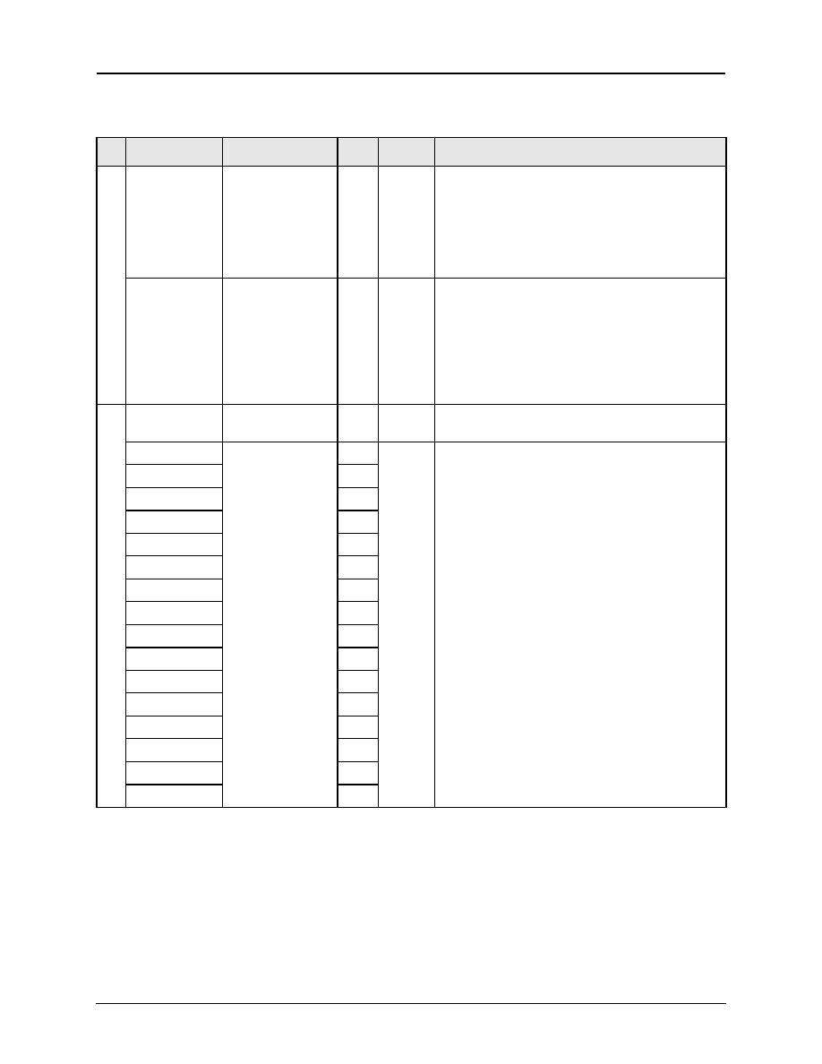
M
ic
ro
In
terf
ac
e
MRdy
Microprocessor
Ready
T2
O
When active high, the current read or write transaction has
been completed. For a read transaction, the data is ready to
be transferred to the microprocessor. For a write
transaction, the data provided by the microprocessor has
been written. This pin is an open drain output for an
external wired OR logic implementation. An external pull-
up resistor is required for this pin.
MicroClk
Microprocessor
Clock
R3
I
An 8–50 MHz clock signal input. The device samples the
microprocessor interface pins (MCS*, MW/R, MAS*,
MicroAddr[10:0], and Microdata[7:0]) on the rising edge
of this signal. The microprocessor interface output pins
(Microdata[7:0], MicroInt*) are clocked on the rising edge
of MicroClk. Note that this clock is required for both
synchronous and asynchronous operations. See note in
E
xt
e
rn
al
Me
mor
y
ExtMemSel
External Memory
Enable
C13
I/PD
When this pin is pulled high, it enables the external
differential delay SRAM bus.
MemData[0]
Differential Delay
Memory Data Bus
T5
I/O/PD
Differential delay SRAM Data Bus. ATM cells extracted
from the Receive data stream are stored in the SRAM for
the purpose of differential delay compensation.
This bus is enabled by pulling the ExtMemSel pin high.
MemData[1]
P6
MemData[2]
R6
MemData[3]
N7
MemData[4]
P7
MemData[5]
N10
MemData[6]
T10
MemData[7]
R10
MemData[8]
P11
MemData[9]
N11
MemData[10]
T11
MemData[11]
R11
MemData[12]
P12
MemData[13]
N12
MemData[14]
A6
MemData[15]
B6
Table 2-5. CX28229 Pin Descriptions (3 of 12)
Pin Label
Signal Name
No.
I/O
Description
相關PDF資料 |
PDF描述 |
|---|---|
| 28230-13 | ATM SEGMENTATION AND REASSEMBLY DEVICE, PQFP208 |
| 28L0138-40R | 1 FUNCTIONS, FERRITE BEAD |
| 28L0138-70R | 1 FUNCTIONS, FERRITE BEAD |
| 28Z551 | TELECOM FILTER |
| 28Z550 | TELECOM FILTER |
相關代理商/技術參數 |
參數描述 |
|---|---|
| 28-22916 | 制造商:CEBEK 功能描述:PRE ASSEMBLED MODULE BOARD PRECISION TIMER 15S-60MIN |
| 28-22918 | 制造商:CEBEK 功能描述:PRE ASSEMBLED MODULE BOARD PRECISION TIMER 0.1-10 SEC |
| 28-22920 | 制造商:CEBEK 功能描述:PRE ASSEMBLED MODULE BOARD PRECISION TIMER 1-99 SEC |
| 28-22922 | 制造商:CEBEK 功能描述:PRE ASSEMBLED MODULE BOARD SEQUENTIAL TIMER 1SEC-3MIN |
| 28-22926 | 制造商:CEBEK 功能描述:PRE ASSEMBLED MODULE BOARD ON DELAY TIMER 1-60 SECOND |
發布緊急采購,3分鐘左右您將得到回復。